Compared with the traditional PC-side system, the image acquisition and processing system based on DSP has the characteristics of low power consumption, convenient carrying and fast processing speed, and is widely used in the field of image acquisition and processing. DSP (Digital Signal Process or) chip, also known as digital signal processor, is a microprocessor device introduced by TI for algorithm processing in digital signal processing systems. The DSP adopts the Harvard structure bus design, the program memory and the data memory are separated, and the value and data access can be performed simultaneously. The DSP also uses pipeline operations to allow multiple instructions to overlap and operate, which can effectively improve instruction execution efficiency. In addition, DSP also has an independent hardware multiplier, which has a very fast speed in processing filtering, convolution, etc. Therefore, DSP is particularly suitable as a core device in image acquisition and processing systems. The video decoding chip of the video acquisition end uses the TVP5150 to convert the acquired analog image signal into a digital image signal.
1 system design overall architecture
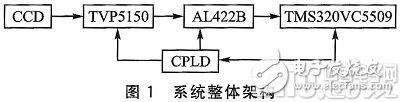
This system is a digital image processing system based on DSP. The overall structure design is shown in Figure 1. First, the CCD camera captures the video image, outputs the standard PAL video signal, and inputs it into the video decoding chip TVP5150. The TVP5150 converts the analog image signal into a digital image signal and sends it to the FIFO. The system uses AL422B. The DSP reads the image data from the FIFO through the EMIF interface and stores it in the memory. The image data is processed by the algorithm in the DSP and transmitted to the PC through the emulator for display. Among them, CPLD is responsible for FIFO read and write pointer reset and read and write enable control.
(First In First Out) is a first-in, first-out data buffer. The difference between FIFO and other memory is that there is no read/write address line, the operation can be very simple, and it can only write data sequentially and read it sequentially. In addition, the FIFO has the following features:
1 Cache continuous data to prevent data loss.
2 The data can be stored centrally, so that the CPU bus avoids frequent operations.
3 Allow the system to perform high-speed DMA operations, that is, directly perform data storage without intervention by the CPU, saving time for using the CPU, and greatly improving the efficiency of the system.
The FIFO is divided into a synchronous FIFO and an asynchronous FIFO. Synchronous FIFO means that the read/write clock must be the same clock, while the asynchronous FIFO can accept one clock to write data, and the other clock can read data, that is, the read/write clocks can be inconsistent and independent of each other.
Since the TVP5150 sends data to the DSP in this system, the write clock of the TVP5150 is different from the read clock of the DSP. The output clock of TVP5150 is 27 MHz, the data bit is 8 bits wide, then the data volume per second is 216 Mbps, and the output clock of DSP is difficult to match the clock frequency of 27 MHz, set to 33 MHz, 8-bit data width, then The maximum transfer rate is 264 Mbps. Obviously, the data transmission amount of the two is different in unit time. If the data is transmitted to each other without any buffer, the system cannot operate synchronously and enters a metastable state, so that the entire system functions. Abnormal. In order to avoid metastable state to achieve high-speed and stable transmission of system data, the system uses asynchronous FIFO as a solution, and uses AL422B as asynchronous FIFO memory with a capacity of 3MB (393 216 bytes & TImes; 8 bits), which can store PAL The information of a frame of graphics. Some of its technical indicators are as follows:
1 supports video signals of VGA, CCIR, NTSC, PAL and HDTV formats;
2 independent read and write operations, can accept different I / O speed;
3 read or write cycle is 20 ns;
4 access time is 15 ns;
5 output enable control;
6 has DRAM self-refresh function;
73.3 V or 5.0 V supply.
The read and write process of AL422B is divided into four steps: write reset, write enable, read reset, and read enable. First reset the write pointer ![]() When writing enable
When writing enable ![]() When low, write data to the write data register on the rising edge of WCK;
When low, write data to the write data register on the rising edge of WCK; ![]()
When high, the write operation is disabled. Then reset the read pointer ![]() , when
, when ![]() When all are low, data is written to the read data register on the rising edge of RCK; otherwise, the read operation is disabled.
When all are low, data is written to the read data register on the rising edge of RCK; otherwise, the read operation is disabled.
2 system hardware design
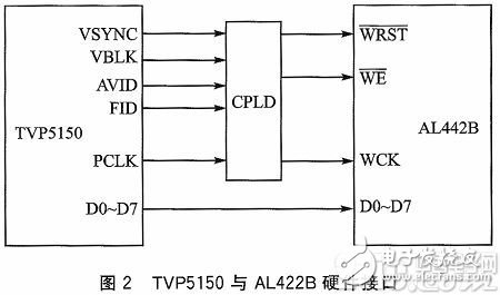
2.1 TVP5150 and AL422B interface implementation
In this system, the data output end of TVP5150 should be connected to the data write end of AL422B, and the data read end of AL422B should be connected to the data input end of DSP. First introduce the hardware connection between TVP5150 and AL422B. The data bus of TVP5150 can be directly connected with the data bus of the write end of AL422B.
The output clock of the TVP5150 needs to be divided by two and phase-shifted for half a clock cycle, and then connected to the write clock WCK of AL422B, because we only need to obtain the grayscale image, which can filter the image of the color part and reduce the amount of data. .
The VSYNC, VBLK, AVID, and FID on the TVP5150 side are logically combined by the CPLD, and then connected to the AL422B write pointer reset WRST and the write enable WE. The specific logical combination will be introduced in the software design section.
The interface between TVP5150 and AL422B is shown in Figure 2.
2.2 Interface implementation of TMS320VC5509A and AL422B
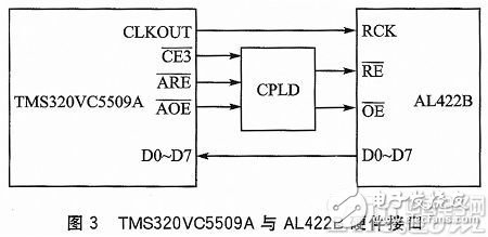
To receive data from AL422B, TMS320VC5509A (hereafter referred to as 5509A) needs to directly connect the read data bus of AL422B with the EMIF data bus interface of 5509A. The 5509A's output clock, CLKOUT, provides the read clock to AL422B. AL422B output enable ![]() And read enable
And read enable ![]() Need to use CPLD to select the external memory chip select signal of 5509A
Need to use CPLD to select the external memory chip select signal of 5509A ![]() , EMIF interface output enable
, EMIF interface output enable ![]() And EMIF interface read enable
And EMIF interface read enable ![]() Make a logical combination and connect. The combinatorial logic is described in the Software Design section. The interface between TMS320VC5509A and AL422B is shown in Figure 3.
Make a logical combination and connect. The combinatorial logic is described in the Software Design section. The interface between TMS320VC5509A and AL422B is shown in Figure 3.
3 system software design
The software part is divided into two parts, namely the programming in the DSP and the combination logic in the CPLD.
3. 1 DSP main program
The program flow chart is shown in Figure 4.
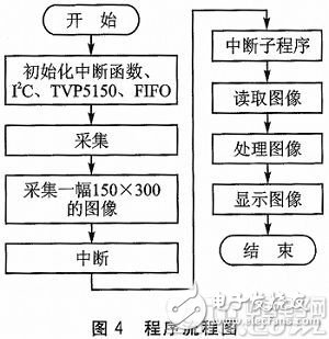
3.1.1 main function initialization
The main function needs to initialize the clock frequency, interrupt function, EMIF external memory interface, I2C bus, TVP5150 video configuration, AL422B write pointer reset.
Among them, AL422B is initialized with GPIO0, GPIO1, GPIO2 of TMS320VC5509A to send logic level to CPLD, then CPLD sends command to control AL422B read and write pointer reset and read and write enable.
In the DSP, first define the directional control register IODIR and pin level register IODATA of the GPIO port, and set the lower 3 bits of the IODIR register to 1, that is, set the direction of GPIO0, GPIO1, and GPIO2 as the output. Then assign the IODA TA register, and send the value of the register to the CPLD through the GPIO port. The CPLD side performs logical combination and writes the pointer to the AL422B reset. ![]() Reset.
Reset.
3.1.2 Initializing TVP5150
The TVP5150 is a video decoder chip that requires an analog input to be a PAL signal that is converted to an 8-bit YUV4:2:2 format digital output signal. The DSP needs to reset the TVP5150 through the GPIO port, similar to the write pointer reset control of AL422B. The DSP also needs to control the registers of the TVP5150 through the I2C bus. The configuration of the TVP5150 registers is as follows:
1 Miscellaneous Control Register: Address 0x03, set to 0x0f.
2 Output and data ratio selection register: Address 0x0d, set to 0x40.
3 Configure the multiplexed pin register: Address 0x0f, set to 0x0a.
4 valid pixel start high register: address 0x11, set to 0x4d.
5 valid pixel start low register: address 0x12, set to 0x02.
6 valid pixel end low register: address 0x13, set to 0xe4.
7 valid pixel end low register: address 0x14, set to 0x02.
After the register configuration, the field blanking signal VBLK, the pixel effective signal AVID, the field sync signal VSYNC, the parity field flag bit signal FID, the output clock SCLK output are valid, the data bus is activated, and the acquired image is cropped into 150 & TImes; 300 image.
After initializing the program, execute a while loop and wait for the interrupt to arrive.
3.1.3 Interrupt function
Since only 150 & TImes; 300 images need to be processed, only 150 × 300 pixels are stored in the FIFO, and an interrupt signal is issued after the memory is full, and the DSP goes to execute the interrupt service routine. The interrupt function first tells the CPLD to reset the read pointer of AL422 B through the GPIO port (the method is similar to the write pointer reset of AL422B, which will not be described here), and the output of AL422B is enabled. ![]() Valid, read enable
Valid, read enable ![]() Valid (specific implementation is described in 3.2). Then the DSP reads the data in the FIFO because the FIFO is expanded outside the DSP.
Valid (specific implementation is described in 3.2). Then the DSP reads the data in the FIFO because the FIFO is expanded outside the DSP. ![]() This space, the address is 0x600000, so the DSP will
This space, the address is 0x600000, so the DSP will ![]() The data in the memory is written into the memory, and the data stored in the memory is processed for subsequent processing.
The data in the memory is written into the memory, and the data stored in the memory is processed for subsequent processing.
Here, the processing algorithm we use is the edge detection method of the image. After the processing is completed, it is displayed in the CCS, and the algorithm processing result is observed.
Finally, a write pointer reset is performed to prepare for the next image acquisition. It should be noted that since the odd and even fields are transmitted separately during the transmission, only a part of the image of the odd field is stored in the FIFO, and the complete image is composed of the odd field and the even field, so the obtained image shows As a result of half-frame image compression, the image is distorted. However, we only observe the processing results of the algorithm, so there is no complete display of the image.
3.2 CPLD procedure
The input signal received by the CPLD has a signal from the GPIO port of the TMS320VC5509A, a field blanking signal VBLK from the TVP5150, a pixel effective signal AVID, a field sync signal VSYNC, and a parity field flag bit signal FID. The output signal of the CPLD has a write enable signal that is supplied to the FIFO. ![]() , write reset pointer signal
, write reset pointer signal ![]() And read reset pointer signals
And read reset pointer signals ![]() And the interrupt signal provided to the TMS320VC5509A
And the interrupt signal provided to the TMS320VC5509A ![]() .
.
When VSYNC changes from high level to low level, the output is a valid video signal, and when VBLK is low and AVID is high, TVP5150 outputs valid video data.
Because the even field is scanned from the middle of a line, if the FID signal is not set, the last acquired image may be an even field signal or an odd field signal. Then, the image displayed in the CCS may be complete. It is also possible to display an image that is reversed left and right, just a half-line image. Therefore, set the FID signal to 0 and collect the signal of the odd field.
CPLD combines these logics to enable AL422B write enable ![]() Effective, TVP5150 outputs video data to AL422B.
Effective, TVP5150 outputs video data to AL422B.
Because to capture a 150x 300 image, you need to set a counter in the CPLD to count the collected pixels. The write clock WCK of AL422B is used as the clock signal of the counter. When the count reaches 45,000, the DSP external interrupt 2 is triggered. Clear the counter to zero.
AL422B is expanded in the DSP ![]() This space, when
This space, when ![]() And EMIF interface output enable signal of TMS320VC5509A
And EMIF interface output enable signal of TMS320VC5509A ![]() When it is low, the output enable signal of AL422B is enabled by the logic combination of CPLD.
When it is low, the output enable signal of AL422B is enabled by the logic combination of CPLD. ![]() . Then when the TMS32 0VC5509A EMIF interface read enable signal
. Then when the TMS32 0VC5509A EMIF interface read enable signal ![]() When low, the AL422B read enable signal is enabled by the logic combination of the CPLD.
When low, the AL422B read enable signal is enabled by the logic combination of the CPLD. ![]() . The logical relationship is as follows:
. The logical relationship is as follows:
![]()
4 Experimental results
Using the designed system for physical image acquisition, Figure 5(a) shows the office seat scene of the acquired laboratory, and Figure 5(b) shows the edge processing of the acquired image using the edge detection algorithm.
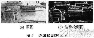
Edge detection highlights the edge features of the image, making it clear to the viewer and contains rich intrinsic information (direction, step properties, shape, etc.).
Conclusion
Set the breakpoint in the DSP simulation software CCS, and after the multiple image acquisition and processing tests, the complete image information can be obtained. The results show that the asynchronous FIFO is used as the data transmission connector between the TVP5150 and the DSP, which can achieve the system preset function and can transmit stably and at high speed.
Lead Free Piezoelectric Elements
The Co-Al Co-doped Barium Titanate
Lead-free Piezoelectric Ceramics was successfully developed by Yuhai company
through repeated experiments. By Researching the influence of Co-Al Co-doping
on the structure and properties of Barium Titanate-based piezoelectric
ceramics, the formulation and preparation technology of Barium Titanate-based
piezoelectric ceramics were optimized. Yuhai`s BaTiO3 was prepared by conventional
solid-phase sintering method, with the piezoelectric constant d33 (>170pC/N),
dielectric loss tgδ≤0.5% and mechanical coupling coefficient Kp≥0.34.
Barium titanate lead-free piezoelectric
ceramics are important basic materials for the development of modern science
and technology, which was widely used in the manufacture of ultrasonic
transducers, underwater acoustic transducers, electroacoustic transducers,
ceramic filters, ceramic transformers, ceramic frequency discriminators, high
voltage generators, infrared detectors, surface acoustic wave devices,
electro-optic devices, ignition and detonation devices, and piezoelectric
gyroscope and so on.
Application: military, ocean, fishery, scientific research,
mine detection, daily life and other fields.
China Patent of Yuhai company`s BaTiO3
Chinese Patent No.: ZL 2011 1
0126758.6
Name: Lead-free Barium Titanate
Piezoelectric Material with Addition of Cobalt and Aluminum
Lead free piezo material BaTiO3
Lead-free Material
Properties
BaTiO3
Dielectric Constant
ɛTr3
1260
Coupling factor
KP
0.34
K31
0.196
K33
0.43
Kt
0.32
Piezoelectric coefficient
d31
10-12m/v
-60
d33
10-12m/v
160
g31
10-3vm/n
-5.4
g33
10-3vm/n
14.3
Frequency coefficients
Np
3180
N1
2280
N3
Nt
2675
Elastic compliance coefficient
Se11
10-12m2/n
8.4
Machanical quality factor
Qm
1200
Dielectric loss factor
Tg δ
%
0.5
Density
Ï
g/cm3
5.6
Curie Temperature
Tc
°C
115
Young's modulus
YE11
<109N/m3
119
Poison Ratio
0.33

Piezo Element,Piezo Ceramic Elements,Piezoelectric Ceramic,Pzt Tubes
Zibo Yuhai Electronic Ceramic Co., Ltd. , https://www.yhpiezo.com