The double integral type A/D converter ICL7107 is an indirect A/D converter. It integrates the input analog voltage and the reference voltage twice, converts the input voltage average into a time interval proportional to it, and then uses the pulse time interval to obtain the corresponding digital output.
It includes an integrator, comparator, counter, control logic, and clock source. The integrator is the heart of the A/D converter. The integrator divides the input signal voltage and the reference voltage twice in one measurement cycle. The comparator compares the output signal of the integrator with a zero level, and the result of the comparison serves as a control signal for the digital circuit.
The standard period Tc of the clock source is used as the standard time for the measurement interval. It consists of two internal inverters and an external RC.
The counter counts the clock pulses of the reverse integration process. Control logic includes dividers, decoders, phase drivers, controllers, and latches. The frequency divider is used to gradually divide the clock pulse to obtain the desired counting pulse fc and the square wave signal fc required for the common electrode of the common anode LED digital tube.
(1) 31/2-bit double integral type A/D converter ICL7107 function and features
1 ICL7107 is a 31/2-bit double-integration A/D converter. It belongs to CMoS LSI. Its maximum display value is ±1999, the minimum resolution is 100uV, and the conversion accuracy is 0.05±1 word.
2 can directly drive the common anode LED digital tube, no need to add a driving device, so that the whole circuit is simplified, use the two 5V power supply, and connect the GND of the 21st pin to the IN of the 30th pin.
3 There is a very stable 2.8V reference power supply between V+ and COM inside the chip. The required reference voltage VREF can be obtained through a resistor divider.
4 Automatic zero adjustment and automatic polarity display can be realized by the internal analog switch. 5 The input impedance is high and there is no attenuation on the input signal.
6 The whole machine is easy to assemble, no need to add active devices, and it can be equipped with a resistor, capacitor and LED common anode digital tube to form a DC digital voltage meter.
7 Low noise, low temperature drift, good reliability and long life. 8 The chip itself consumes less than 15mw (excluding LEDs).
9 There is no special decimal point drive signal. When using, the LED common anode digital tube common anode can be connected to V+. 10 for convenient function check.
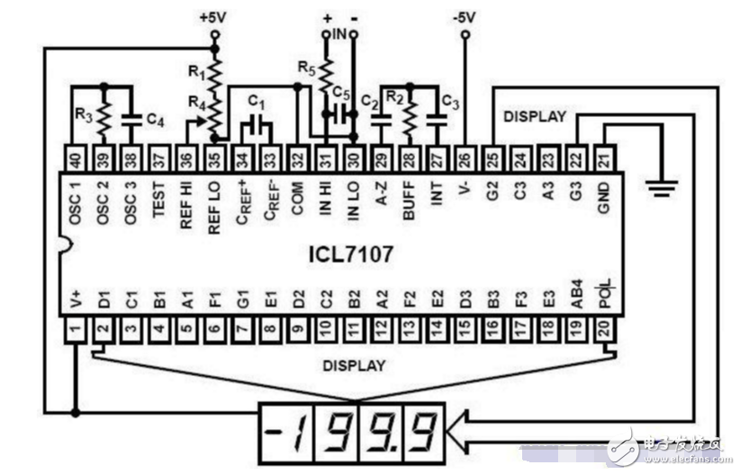
Figure 1 ICL7107 pin diagram and typical circuit
(2) ICL7107 pin function
Au-gu, aT-gT, aH-gH: drive signals for single, ten, and hundred strokes, respectively, followed by corresponding stroke electrodes of one, ten, and hundred LED displays.
Bck: Thousand strokes of driving signals. The corresponding stroke electrode of the thousands of LEO displays. PM: The driving end of the common electrode on the back of the liquid crystal display, referred to as the back electrode.
Oscl-OSc3: The terminal of the clock oscillator, an external resistor or a quartz crystal oscillator. The choice of capacitance from pin 38 to pin 40 is determined according to the following formula: Fosl = 0.45/RC
COM: The analog signal common terminal, referred to as "analog ground", is generally connected to the negative terminal of the input signal and the negative terminal of the reference voltage. TEST: Test terminal, which is connected to the common ground of the logic circuit through a 500 ohm resistor, so it is also called "logic ground" or "digital ground". VREF+ VREF- : Positive and negative of the reference voltage. CREF: External reference capacitor terminal.
INT: 27 is an integrating capacitor. It is necessary to select the components IN+ and IN- which have a small temperature coefficient and do not cause the input voltage of the integrator to drift. The analog input terminals are respectively connected to the positive and negative terminals of the input signal.
AZ: The inverting input of the integrator and comparator is connected to the auto-zeroing capacitor CAz. If the application is at 200mV full scale, 0.47μF is used, while the 2V full scale is 0.047μF.
BUF: Buffer amplifier output, connected to the integral resistor Rint. The output stage has an idling current of 100μA, and the buffer and integrator can supply 20μA of drive current. From this pin, a Rint is connected to the integrating capacitor. The value is 47K at full scale 200mV, and 2V full scale. Then use 470K.
Design of interface between ICL7107 and 8031The ICL7107 is a 3-bit, half-double-slope integral A/D converter designed by Intersil for digital instrumentation. It requires only a small number of common components to form a peripheral circuit, which can be made into a sophisticated digital instrument. It has the characteristics of high resolution and strong anti-interference ability, and is widely used for its high performance and price ratio. It can directly drive the LED digital block, but there is no corresponding BCD code output, and there is no A/D conversion status flag output, so it can not access the microcomputer system for field data collection and processing. This paper presents an extremely simple The method makes the ICL7107 interface with the 80 31, thus extending its functionality and scope of use.
Analysis of interface conditions
The I/C conversion cycle of the ICL7107 is divided into three phases: the integral INT) phase, the elimination integral (DE) phase, and the autozero (AZ) phase, as shown in Figure 1.
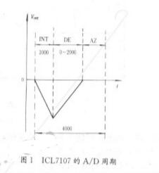
The time of one conversion cycle is 4000 count pulse cycles. The integration phase integrates the input voltage within the specified 1000 count pulse cycles. The elimination integration phase is to reversely integrate the reference voltage and count from the internal counter to the integral. The output is 0. The count value of this time is linearly proportional to the input voltage. The range is 0~2000 times for automatic zero adjustment. When the input voltage is 0~2000, the auto zero time is It varies within the range of 3000-1000 count pulse periods. The frequency of this internal count pulse is divided by 4 of the 7107 clock oscillation frequency.
If you can find - a status signal that can mark the A/D conversion cycle, using it as the interface's handshake signal, there is a basis for implementing the interface. According to the internal structure principle of 1CL.71017, the signal waveform shown in Figure 2 can be found at pin No. 34 (CREF').
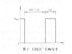
In both stages of INT and DE, this pin is low during the AZ phase, and the level of this pin is the reference. We can convert this signal to a TTL level compatible with the 8031. In this way, the interface hardware circuit shown in FIG. 3 can be drawn by using the same method as the literature.
Interface design and implementation
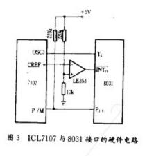
In the circuit of Fig. 3, only three port lines of 8031 ​​are used, and the To port is set to the counting mode 1J, and INTO and P1.0 respectively receive the level-converted A/D conversion state signal and the positive and negative polarity signals. With the digital instrument composed of ICL710, the polarity of the live input signal is generally determined. So P. The connection of the line can often be omitted. In the program, set GATE=1, so that the action of INTo is the gate of To. During the INTO=1, To counts the clock of 7107, and stops when INTo=0. Setting external interrupt 0 is the edge trigger. The reading and processing of the T count value is scheduled in the interrupt service routine. Since the internal count pulse of the ICL7107 is divided by 4 of its clock period, the binary result of the A/D conversion is obtained by dividing the count value of T by 4 and subtracting the 1000 count values ​​inherent in the integration stage.
The reference procedure is as follows:
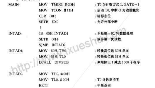
The interface method implemented in this paper is in the counting process of ICL's on-chip timing integration and fixed-slope elimination integration. The counter counts its clock pulse by the timing of 801. The count value is divided and the timing integral is subtracted. The inherent count value is the binary result of the 3-bit half-A/D converter. The internal count value of 710 is only for decoding and display, while the 801 timing, the result of the counter reading is the field data of the intelligent instrument. Both do their best and perform their duties. The conversion result read by the 8031 ​​is strictly consistent with the 710-driven LED display. This interface method is also applicable to other ICL A/D converters with display drivers, such as 7106.7116.7117.7126.7129 and 7137.
3.2v12-30Ah Lithium Battery Cells
3.2v12-30Ah Lithium Battery Cells,3.2v12-30Ah Lithium Battery Cells price,3.2v12-30Ah Lithium Battery Cells product
Jiangsu Zhitai New Energy Technology Co.,Ltd , https://www.zt-tek.com