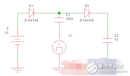
The basic principle of the charge pump is that the charging and discharging of the capacitor adopt different connection modes, such as parallel charging, series discharging, series charging, parallel discharging, etc., to realize voltage conversion functions such as boost, buck, and negative voltage.

The figure above shows the double boost charge, which is the simplest charge pump circuit. The output of V2 is a square wave signal. When V2 is low level, V1 charges capacitor C2 through D1, C1 and V2, and the voltage across C2 is positive and negative. When V2 is high level output, V2 output voltage. Superimposed on the voltage across C1, power is supplied to the load through D3 and C2 is charged. If the diode drop is ignored, the voltage across C2 is Vo = V2 + V1, where V2 is the high level output voltage of voltage source V2.
Since the core part of the whole working process of the charge pump is the charge and discharge process of the capacitor, the most important formula is the charge and discharge formula of the capacitor: I*T=ΔV*C, where T is the charge and discharge cycle of the capacitor, and ΔV is the cycle of each charge and discharge. The voltage across the capacitor fluctuates and I is the charge and discharge current.
The charge pump can realize functions such as step-up, step-down, and negative voltage in a very simple circuit, so the circuit expands the low-power circuit in various occasions.
2, the role of charge pump in the circuit1. Charge pump in power circuit
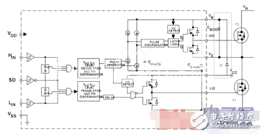
A very broad use of charge pumps is to provide floating drive voltage to the upper arm in a half-bridge circuit composed of N-channel MOSFETs. The typical connection is shown in the figure below. The diode D and capacitor Cboot in the red frame and the lower arm T1 of the half bridge in the main circuit form a charge pump. When the lower arm T1 of the half bridge is turned on, Vcc charges the capacitor Cboot through D and T1; when T1 turns off T2 is turned on, Cboot provides the upper arm T2 with the Vgs voltage necessary for the MOSFET to turn on. This is due to the position of T2 in the circuit. When T2 is turned on, if the turn-on voltage drop Vds is ignored, the source voltage of T2 is Vs=Vr, so if you want to saturate, turn on the T2 gate. The drive voltage needs to meet Vg=Vr+Vgs. For power N-channel MOSFETs, Vgs usually need about 15V. Charge pumps meet this design requirement with few components and are therefore widely used in such applications.

Although the bootstrap type charge pump described in the above figure (using the lower arm of the half bridge as part of the charge pump) makes the circuit design very simple, there are some limitations in the actual use, such as the turn-on timing of the bridge arm and There is a limit to the ratio of air. Therefore, in some applications where the requirements are relatively high, the charge pump of the drive type is used, that is, the charge pump circuit and the drive waveform are separated from the main power circuit, and an external circuit is used to form the charge pump. Although such a structure is slightly more complicated than the bootstrap driving circuit, it overcomes some problems of the bootstrap driving circuit and is widely used in some occasions.
2. Boost and negative voltage in RS-232 level conversion
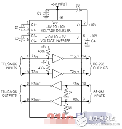
Another very broad application of charge pumps is to provide RS-232 compliant supply voltages for level-shifting chips. The level-shifting chip is usually powered by a single 3.3V or 5V power supply, while the RS232 level standard requires a logic level of "1" from -3 to -15V and a logic level of "0" from +3 to +15V. Therefore, the RS232 conversion chip not only needs to complete level conversion, but also provides power conversion that meets the requirements.
The following figure shows a typical block diagram of the RS232 level-shifting chip. First, a boost charge pump is used to double-voltage boost the +3.3V or 5V input power supply, and then a double-voltage boost is applied by a negative-charge pump. The power output is converted to a negative voltage.

Modular Switch And Socket,Gm Modular Switches,Gm Electrical Switches,Modular Switches For Home
ZHEJIANG HUAYAN ELECTRIC CO.,LTD , https://www.huayanelectric.com