Transistor is one of the most important electronic components. John Bardeen, an American physicist who successfully produced the world's first semiconductor triode, and his colleague Brattain won the Nobel Physics. prize. The triode's housekeeping ability is to control large currents with a small current, which is similar to the four or two of the martial arts.
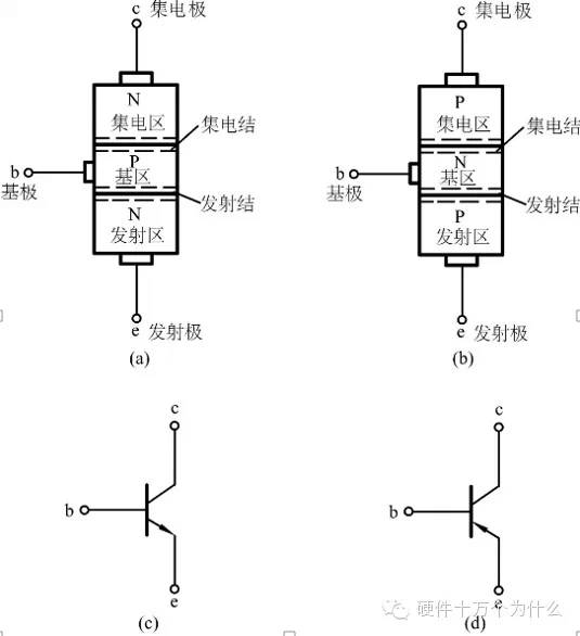
The figure below shows the structure and circuit diagram symbols of two types of triodes NPN and PNP.
Positive positive [ˈpɒzətɪv]
Negative negative [ˈnegətɪv]
Many beginners think that a triode is a simple make-up of two PN junctions. This idea is wrong, the combination of two diodes does not form a triode. Let's take the NPN transistor as an example (see Figure 2). The two PN junctions share a P-region, which is extremely thin, only a few micrometers to tens of micrometers. The PN junctions are organically combined into an indivisible whole. They are interconnected and interact with each other, making the triode completely different from the characteristics of two separate PN junctions. The triode forms a base current, a collector current, and an emitter current under the action of an applied voltage, becoming a current amplifier component.
The current amplification of the triode is related to its physical structure. The physical process carried out inside the triode is very complicated, and beginners do not need to delve into it for the time being. From an application point of view, the triode can be thought of as a current divider. After a triode is fabricated, the proportional relationship between its three currents is generally determined (see Figure 3).
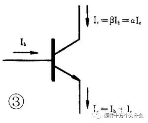
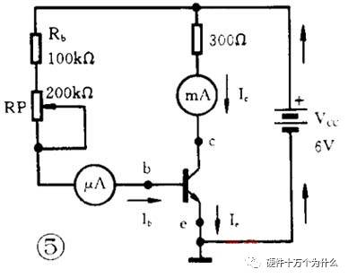
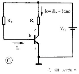
β and α are called the current distribution coefficients of the triode, and the β value is familiar to everyone, and it is called the current amplification factor. One of the three currents changes, and the other two currents change proportionally. For example, the amount of change in the base current ΔI b = 10 μA , β = 50. According to the relationship of ΔI c = βΔI b , the amount of change in the collector current ΔI c = 50 × 10 = 500 μA, and current amplification is realized. The triode itself does not turn a small current into a large current. It only serves as a control to control the power supply in the circuit and provides three currents I b , I c and I e to the triode in a determined ratio. For ease of understanding, we also use water flow analogy (see Figure 4). This is a thick and thin water pipe. The thick pipe is equipped with a gate. The gate is controlled by the amount of water in the thin pipe. If there is no water flow in the thin tube, the gate in the thick tube will close. The larger the amount of water injected into the thin pipe, the larger the gate is opened, and the more water flows through the thick pipe accordingly, which reflects the principle of “small control with small control and strong control with weak controlâ€. As can be seen from the figure, the water of the thin tube merges with the water of the thick tube at a lower end in a tube. The base b, the collector c and the emitter e of the triode correspond to the tubes in which the thin tubes, the thick tubes and the thicknesses of Fig. 4 meet. The circuit is shown in Figure 5. If a certain voltage is applied to the transistor, currents I b , I c and I e are generated. Adjusting the potentiometer RP changes the base current I b , I c also changes. Since I c = βI b , a small I b controls I c which is β times larger than it. I c is not generated by the triode and is supplied by the power supply VCC under the control of I b , so the triode acts as an energy converter.

As shown in the figure, assume that the transistor has β=100, RP=200K, at this time Ib=6v/(200k+100k)=0.02mA, Ic=βI b=2mA, when RP=0, Ib=6v/100k=0.06mA , Ic = βI b = 2 mA. Both of the above states are in accordance with Ic = βI b, and we say that the triode is in the "amplification zone". Suppose RP=0, Rb=1k. At this time, Ib=6v/1k=6mA is calculated as Ic=βI b, and Ic should be equal to 600mA. In fact, due to the existence of 300 ohm current limiting resistor (Rc) in the figure, the actual Ic = (6v / 300) ≈ 20mA, at this time, Ic ≠βI b, and, Ic is no longer controlled by Ib, that is, in the "saturation zone", when RP and Rb are large to a certain extent, Ube < dead zone voltage (Si tube is about 0.5V, tube is about 0.3) At this time, the junction is in a non-conducting state, and Ib=0, then Ic=0, which is in the "cut-off area".
From the perspective of “zooming inâ€, we hope that the larger the β value, the better. However, when the triode is connected to the common emitter amplifying circuit (Fig. 6), a harmful leakage current is always generated from the collector c to the emitter e of the tube, which is called the penetration current I ceo, and its magnitude is similar to the β value. In proportion, the larger the β value, the larger I ceo is. I ceo This parasitic current is not controlled by I b but becomes part of the collector current I c , I c = βI b + I ceo . It is worth noting that I ceo has a close relationship with temperature. As the temperature rises, I ceo sharply increases, which destroys the stability of the operation of the amplifier circuit. Therefore, when selecting a triode, the larger the β, the better. It is generally recommended to take a silicon tube β of 40 to 150 and a fistula of 40 to 80.
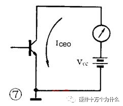
At normal temperature, the penetrating current of the fistula is relatively large, generally from tens of microamperes to hundreds of microamperes, and the penetration current of the silicon tube is relatively small, generally only a few microseconds to several microamperes. Although I ceo is not big, it has a close relationship with temperature. They follow the so-called “doubling ruleâ€, which means that for every 10 °C increase in temperature, I ceo is about doubled. For example, when a tube is at a normal temperature of 20 ° C, I ceo is 20 μA. When the temperature of the tube rises to 50 ° C during use, I ceo increases to about 160 μA. The circuit for measuring I ceo is very simple (Figure 7), the base of the triode is open, the power supply V CC (6V) is connected between the collector and the emitter, and the ammeter connected in series in the circuit (a 0.1mA block in the multimeter can be used) The indicated current value is I ceo .
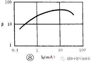
Strictly speaking, the beta value of a triode is not a constant constant. In actual use, adjust the collector current I and β of the triode to change (Figure 8). In general, when I c is small (for example, several tens of microamperes) or large (that is, close to the maximum allowable current I CM of the collector), the β value is relatively small, and a small power tube is in a relatively wide range of 1 mA or more. The β value is relatively large, so when students debug the amplifier circuit, it is necessary to determine the appropriate operating current I c to obtain the best amplification state. In addition, the β value is also the same as the other parameters of the triode, and has a close relationship with temperature. As the temperature rises, the β value becomes correspondingly larger. For every 1 °C increase in temperature, the β value increases by 0.5% to 1%.
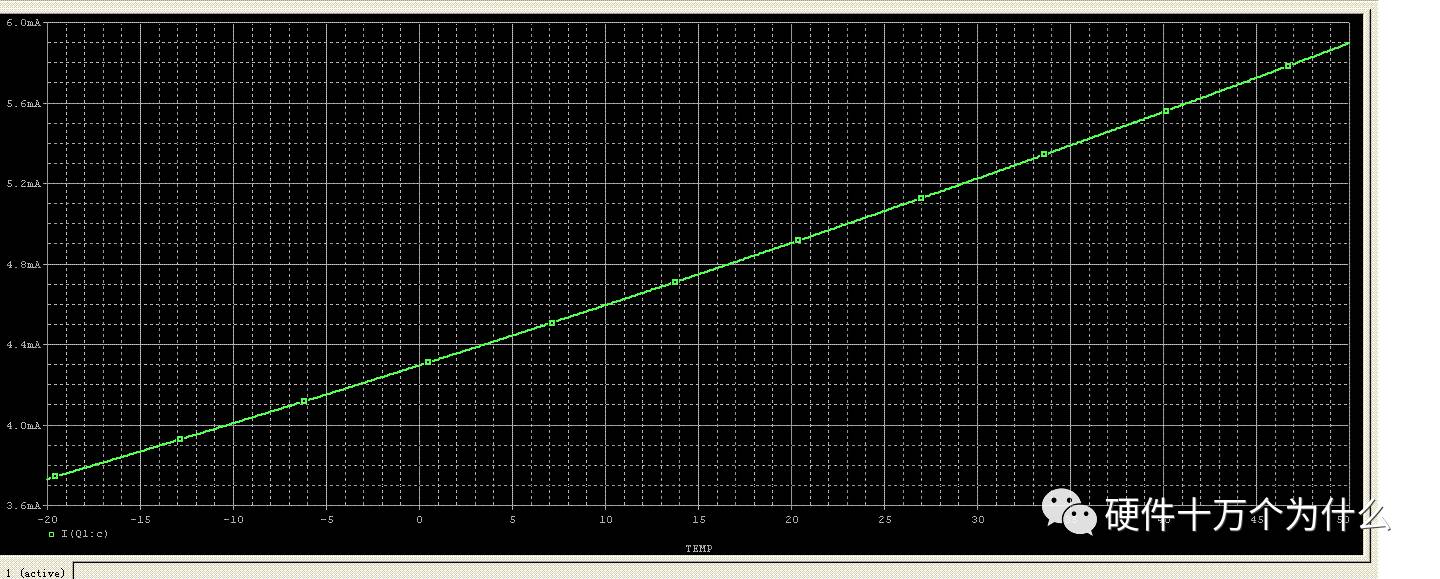
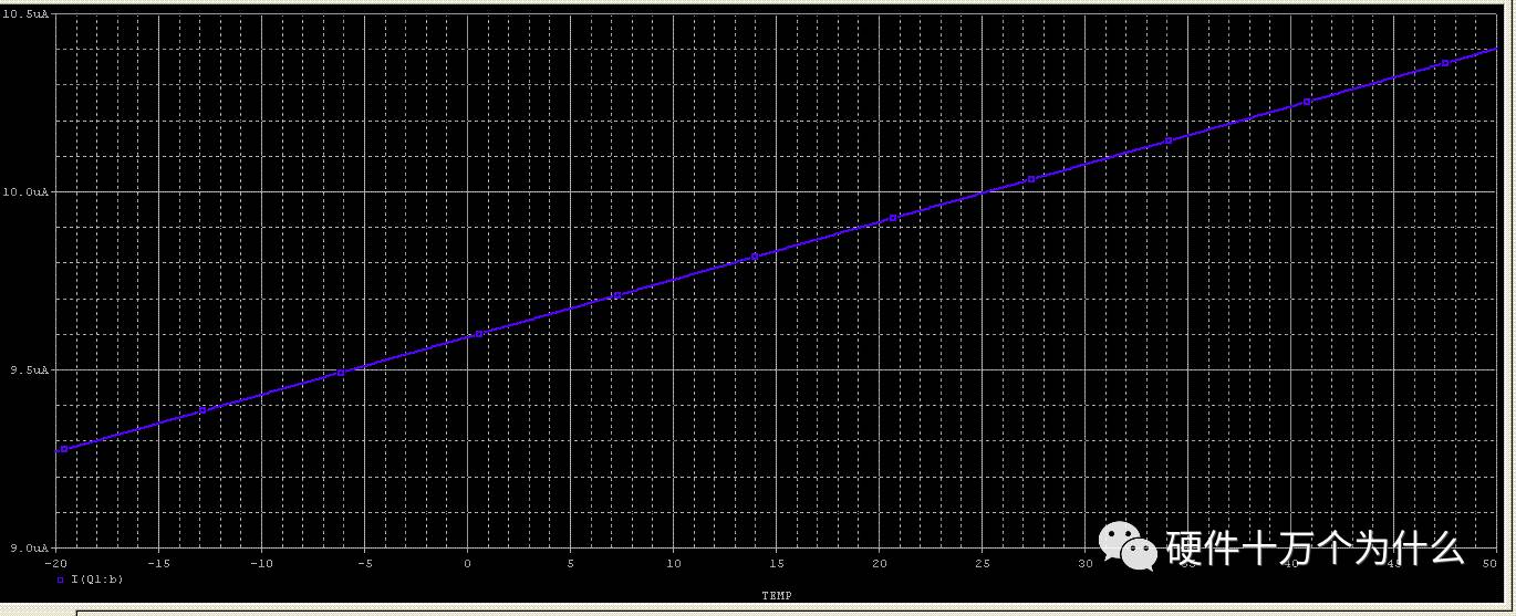
Device is BC847
When the temperature is -20 ° C, Ic is equal to 3.745 mA, and when the temperature is 50 ° C, Ic is equal to 5.897 mA.
Change from -20 ° C to 50 ° C
ß change = (5.897 mA - 3.745 mA) / 3.745 mA = 57.46%.
ß is linear
Rate of change = 57.46% / 70 ° C = 0.812% / ° C.
When using 40239, the ß change is 67.24%.
When the temperature is -20 °C, IB is equal to 9.27uA and the temperature is 50 °C.
IB is equal to 10.4 uA.
Change from -20 ° C to 50 ° C
IB change = (10.4uA-9.27uA) / 9.27uA = 12.19%.
IB changes linearly
The IB change rate = 12.19% / 70 ° C = 0.174% / ° C.
The triode has a limit parameter called the collector maximum allowable current, expressed in I CM. I CM is often called the rated current of a triode, so people often mistakenly exceed the I CM value, which will burn out the tube due to overheating. In fact, the I CM value is specified to avoid excessive β degradation when the collector current is too large. Generally, the collector current when the β value is reduced to about half of its maximum value is determined as the maximum allowable current of the collector.
I CM.
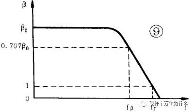
The current amplification factor β of the triode is also related to the operating frequency of the circuit. In a certain frequency range, it can be considered that the β value does not change with frequency (Fig. 9), but when the frequency rises above a certain value, the β value will decrease significantly. In order to ensure that the triode still has sufficient amplification capability at high frequencies, it is stipulated that when the frequency is raised to reduce the β value to 0.707 times the low frequency (1000 Hz) value β 0 , the corresponding frequency is called the β cutoff frequency. f β is indicated. f β is the maximum operating frequency allowed when the triode is connected to the common emitter circuit.
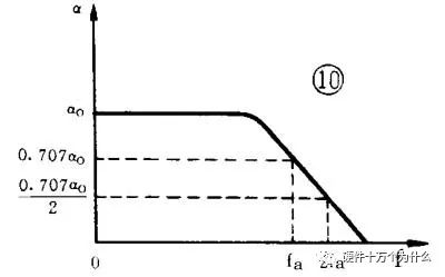
The triode beta cutoff frequency fβ is measured when the triode is connected to a common emitter amplifying circuit. If the triode is connected to a common base circuit, as the frequency increases, the value of the current amplification factor α ( α = I c / I e ) drops to 0.707 times the low frequency ( 1000 Hz ) value α o , and the corresponding frequency is called The α cutoff frequency is denoted by f α (Fig. 10). f α reflects the frequency limit of the common base of the triode. In the triode product line, the low frequency tube and the high frequency tube are often divided according to the size of f α . According to the national regulations, f α < 3MHz is a low frequency tube, and f α > 3MHz is a high frequency tube.
When the frequency is higher than the f β value, the frequency will continue to increase, and the β value will decrease until β = 1, and the triode loses its amplification capability. To this end, it is stipulated that at high frequencies, the frequency corresponding to β = 1 is called the characteristic frequency and is denoted by f T . f T is often used as an important parameter to mark the frequency characteristics of the triode. When selecting a triode, the characteristic frequency f T of the tube should be 3 to 5 times higher than the actual operating frequency.
The physical meaning of f α and f β is the same, except that the amplification circuit is connected differently. Theoretical analysis and experiments can prove that the f β value of the same triode is much smaller than the f α value, and the relationship between them is f β =( 1 - α ) f α
This shows that the limit operating frequency of the common emitter circuit is much lower than that of the common base circuit. Therefore, most of the high-frequency amplification and oscillation circuits use a common base connection.
Lecture first
To illustrate the problem naturally, choose the right point. The principle of triodes begins with the principle of diodes. The structure and principle of the diode are very simple, and a PN junction inside has unidirectional conductivity, as shown in diagram B. It is obvious that the diode is in a reverse biased state and the PN junction is turned off. We must pay special attention to the cut-off state here. In fact, when the PN junction is turned off, there will always be a small leakage current, that is, the PN junction always has a reverse-off phenomenon, and the unidirectional conductivity of the PN junction. Not 100%.
Why would such phenomenon happen? This is mainly because the P region always has a very small number of intrinsic carriers "electrons" in addition to the majority carrier "holes" due to "doping". The same is true for the N region, and in addition to the majority carrier electrons, a very small number of carrier holes are present. When the PN junction is reverse biased, the majority of carriers capable of positive conduction are pulled toward the power supply, so that the PN junction becomes thicker, and most carriers can no longer assume the function of current-carrying conduction through the PN junction. Therefore, the formation of leakage current at this time mainly depends on minority carriers, and minority carriers are conducting electricity. When reverse biased, minority carriers can easily reverse the PN junction to form leakage current under the action of the power supply. The leakage current is only small because the number of minority carriers is too small. It is obvious that the magnitude of the leakage current at this time mainly depends on the number of minority carriers. If you want to artificially increase the leakage current, just think of ways to increase the number of minority carriers when reverse bias. Therefore, as shown in Fig. B, if the number of minority carriers can be artificially increased in the P zone or the N zone, the natural leakage current will increase artificially. In fact, the principle of photodiodes is this. The photodiode has the same unidirectional conductivity as a conventional photodiode. Therefore, the photodiode should be operated with a reverse voltage as shown. When there is no light, there is also a small reverse saturation leakage current in the circuit, generally 1 × 10 -8 - 1 × 10 -9A (called dark current), which is equivalent to the photodiode cutoff; when there is light The vicinity of the PN junction is bombarded by photons. The valence electrons trapped in the semiconductor absorb the photon energy and are fired to generate electron-hole pairs. The number of these carriers has little effect on the majority carriers, but on the P region and In the case of minority carriers in the N region, the concentration of minority carriers is greatly increased. Under the action of the reverse voltage, the reverse saturation leakage current is greatly increased to form a photocurrent, which varies with the intensity of the incident light. And the corresponding changes. When the photocurrent passes through the load RL, a voltage signal that changes with the human light is obtained across the resistor. This is how the photodiode completes the electrical function conversion. 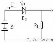
The photodiode works in the reverse bias state, because the illumination can increase the number of minority carriers, and thus the illumination will cause a change in the reverse leakage current. People use this principle to make a photodiode. Since the increase in leakage current is artificial at this time, the increase in leakage current can easily be artificially controlled.
Emphasize a conclusion:Speaking of this, we must focus on the role and nature of majority and minority carriers when PN junctions are positive and reverse biased. The positive partial current is the majority carrier current carrying conductivity, and the reverse bias is the minority carrier current carrying conductivity. Therefore, the positive bias current is large, the reverse bias current is small, and the PN junction exhibits unidirectional electrical properties. In particular, it is important to note that it is easy for a minority carrier to pass through the PN junction in reverse bias, even if the majority of carriers are positively passing through the PN junction. why? It is known that there is an internal electric field generated by the mutual diffusion of majority carriers in the PN junction, and the direction of action of the internal electric field always blocks the positive passage of the majority carriers. Therefore, most carriers pass through the PN junction. It is necessary to overcome the effect of the internal electric field, and an applied voltage of about 0.7 volt is required, which is the gate voltage of the PN junction forward conduction. In the case of reverse bias, the internal electric field is strengthened under the action of the power source, that is, the PN junction is thickened. When the minority carrier reversely passes through the PN junction, the direction of the internal electric field is the same as the direction of the minority carrier passing through the PN junction, that is, It is said that the internal electric field at this time will not only hinder the reverse passage of minority carriers, but may even help. This leads to the conclusion we have said above: it is easy for a minority carrier to pass through the PN junction in reverse bias, even if the majority of carriers are positively passing through the PN junction. This conclusion can well explain the "problem 2" mentioned above, which is the saturation state of the triode to be mentioned in the subsequent content of the textbook. In the saturated state of the triode, the collector potential is very low or even close to or slightly lower than the base potential, and the collector junction is at zero bias, but there is still a large collector current reverse current Ic.
Natural transition: Continue to discuss Figure B, the reverse bias state of the PN junction. By controlling the number of minority carriers generated by illumination, the amount of leakage current can be artificially controlled. In this case, people naturally think about whether the control method can be changed. Instead of lighting, the method of electric injection is used to increase the number of minority carriers in the N zone or the P zone, thereby realizing the leakage current of the PN junction. control. That is, instead of "light", the "electric" method is used to control the current (Note 2). Next, we will focus on the P area. The minority carriers in the P area are electrons. To inject electrons into the P area by means of electric injection, the best method is to add a special process under the P area as shown in Figure C. An N-type semiconductor (Note 3).
Figure C shows the original shape of the NPN-type transistor. The names and functions of the corresponding parts are identical to those of the triode. For the convenience of discussion, we will directly use the names corresponding to the triodes (such as "emission junction", "collector", etc.) for the names of the various parts shown in Figure C. Referring again to the schematic diagram C, the electrons in the N-type semiconductor of the lowermost emitter region are present as a large number of carriers, and, as shown in FIG. C, electrons of the emitter region are injected or transmitted to the P region (base). Zone) is very easy, as long as the emitter junction is forward biased. Specifically, it is sufficient to add a sufficient positive gate voltage (about 0.7 volts) between the base and the emitter. Under the action of the applied gate voltage, the electrons in the emitter region are easily injected into the base region, thus achieving a quantitative change in the number of minority carriers "electrons" in the base region.
Formation of collector current Ic:As shown in Figure C, after the emitter junction is positively biased, the majority of the carriers in the emitter region, electrons, are easily emitted into the base region by the applied voltage. Once these carriers enter the base region, their properties in the base region (P region) are still of minority carrier nature. As mentioned earlier, minority carriers are easily reversed through the PN junction in a reverse biased state, so these carriers - electrons can easily pass upward through the collector junction in the reverse bias state to reach the collector The region forms a collector current Ic. It can be seen that the formation of the collector current does not necessarily depend on the high potential of the collector. The magnitude of the collector current is more dependent on the emission and injection of carrier-to-base regions in the emitter region, depending on the extent of such emission and implantation. The degree of emission injection of such carriers has little to do with the level of the collector potential. This is a natural reason why the collector current Ic is independent of the magnitude of the collector potential Vc in the amplified state. In the amplified state, Ic is not controlled by Vc. The role of Vc is mainly to maintain the reverse bias state of the collector junction, so as to meet the external circuit conditions required for the triode amplification. For Ic, we can also make the following conclusion: The essence of Ic is the "small child" current, which is the artificially controlled collector junction "leakage" current realized by electron injection, so it can easily reverse the collector junction.
The relationship between Ic and Ib: It is obvious that for the internal circuit of the triode, Figure C and Figure D are completely equivalent. Figure D is a schematic diagram of the triode current amplification principle commonly used in textbooks. Looking at Figure D, and then discussed above, the collector current Ic is independent of the magnitude of the collector potential Vc, depending primarily on the extent of carrier injection into the base region of the emitter region.
Through the above discussion, it is now understood that in the current amplification state, the main internal current of the triode is formed by the carrier electrons passing through the base region from the emitter region to the collector region through the triode. That is, the current Ic passing through the triode is mainly a flow of electrons. This through-flow of electrons is very similar to historical electronic transistors. Figure E, Figure E is a schematic diagram of the principle of an electronic triode. The principle of current amplification of an electronic triode can be explained naturally because of its intuitive image.
As shown in Fig. E, it is easy to understand that the fixed proportional relationship between the electron transistors Ib and Ic mainly depends on the configuration of the gate (base) of the electron tube. When the external circuit conditions are met, the triode operates in an amplified state. In the amplified state, the current through the tube is primarily the flow of electrons from the emitter through the gate to the collector. When the electron flow passes through the gate, it is obvious that the gate will intercept it, and there is a problem of the intercept ratio when the flow is intercepted. The size of the intercept ratio is mainly related to the density of the gate. If the gate is dense, its equivalent intercept area is large, the intercept ratio is naturally large, and the intercepted electron flow is much. On the contrary, the interception ratio is small, and the intercepted electron flow is less. The electron flow intercepted by the gate is actually the current Ib, and the rest of the electron flow passing through the gate to the collector is Ic. As can be seen from the figure, as long as the structural size of the gate is determined, the intercept ratio is determined, that is, the ratio of Ic to Ib is determined. Therefore, as long as the internal structure of the tube is determined, the value is determined and the ratio is fixed. It can be seen from this that the beta value of the current amplification factor is mainly related to the density of the gate. The denser the gate, the larger the cutoff ratio, and the lower the corresponding β value, the smaller the gate is, the smaller the cutoff ratio is, and the higher the corresponding β value.
In fact, the current amplification relationship of the transistor is similar to that of an electronic triode. The base of the transistor is equivalent to the gate of the electron triode, and the base is equivalent to the grid, except that the grid of the transistor is dynamic and invisible. In the amplified state, when the electron flow through the entire tube passes through the base region, the base region acts similarly to the grid of the electron tube, and the electron flow is intercepted. If the base region is made thin, the doping degree is low, and the number of holes in the base region is small, the hole-to-electron interception flow is small, which is equivalent to the grid of the electron tube being relatively sparse. On the contrary, the interception traffic will be large. It is obvious that this cutoff ratio is determined as long as the internal structure of the transistor is determined. Therefore, in order to obtain a large current amplification factor, the β value is sufficiently high, and the base region is often made thin in the fabrication of the triode, and the doping degree is also controlled to be low.
Unlike an electron tube, the interception of a transistor is mainly achieved by a positively charged "hole" distributed in the base region and a negatively charged "electron" neutralization in the through electron flow. Therefore, the effect of interception depends mainly on the number of holes in the base. Moreover, this process is a dynamic process, "holes" are constantly neutralized with "electronics", and "holes" are constantly supplemented by external power sources. In this dynamic process, the equivalent total number of holes is constant. The total number of holes in the base region depends mainly on the degree of doping and the thickness of the base region. As long as the transistor structure is determined, the total amount of holes in the base region is determined, and the corresponding dynamic total amount is determined. Thus, the cut-off ratio determines that the value of the current amplification factor of the transistor is a fixed value. This is why there is a fixed proportional relationship between the currents Ic and Ib of the triode in the amplified state.
Explanation of the cutoff state:The proportional relationship indicates that the current Ic is controlled by the current Ib at a fixed ratio in the amplified state, and this fixed control ratio mainly depends on the internal structure of the transistor.
For an off state where Ib is equal to 0, the problem is simpler. When Ib is equal to 0, it means that the external voltage Ube is too small, and the gate voltage value of the emitter junction is not reached. The emitter region does not have the carrier "electron" injected into the base region, so there is neither current Ib nor current. It is even less likely that there is a current Ic. In addition, it is easier to draw conclusions from the purely mathematical current amplification formula, Ic = βIb, Ib is 0, and it is clear that Ic is also zero.
Transistor package and pin
The package form of the triode refers to the shape parameter of the triode, that is, the outer casing for mounting the semiconductor triode. In terms of materials, the package form of the triode is mainly in the form of metal, ceramic and plastic; in terms of structure, the package of the triode is TO×××, and ××× indicates the shape of the triode; the assembly method has through-hole insertion (through-hole type), surface Mounting (sMD type) and direct mounting; pin shapes are long lead wire, short lead or leadless mounting. Commonly used triodes are available in TO-92, TO-126, TO-3, TO-220TO, etc.
Domestic transistors are classified into nearly 30 types and dozens of specifications according to the original standard. The outline structure and specifications are represented by letters and numbers, such as TO-162 and TO-92. The shape and dimensions of the transistor are shown in Figure 1.
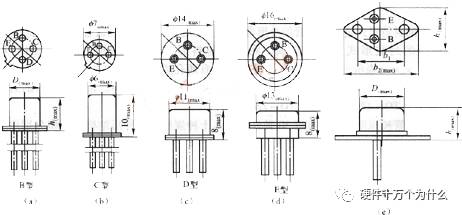
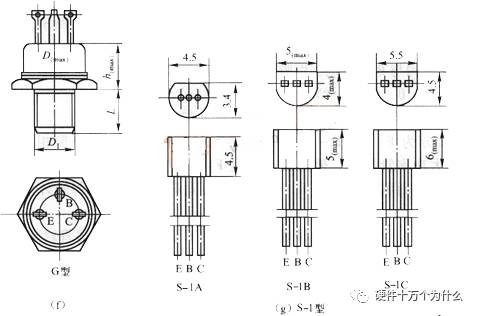
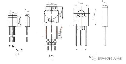
Figure 1 Shape and size of the transistor
Package
Metal package
(1) Type B: Type B is divided into six specifications of B-1, B-2, ..., B-6. It is mainly used for high frequency small power transistors below 1W and below 1W, among which B-1 and B-3 The type is most commonly used. Pin arrangement: the bottom of the tube is facing itself, starting from the tube key, in the clockwise direction, E, B, C, D (grounding pole). The package outline is shown in Figure 2(a).
(2) Type C: The pin arrangement is the same as the B type, and is mainly used for low power. The package outline is shown in Figure 2(b).
(3) Type D: The outer structure is the same as the B type. Pin arrangement: the bottom of the tube is facing yourself, the bottom surface of the isosceles triangle is facing downward, and the clockwise direction is E, B, C. The package outline is shown in Figure 2(c).
(4) Type E: The pin arrangement is the same as the D type, and the package outline is shown in Figure 3(d).
(5) F type: This type is divided into five specifications of F-0 and F-1 to F-4. Each specification has the same shape and different dimensions. It is mainly used for low-frequency high-power tube packaging. The most used is F-2. Type package. Pin arrangement: the bottom of the tube is facing yourself, the face of the small isosceles triangle is facing down, the left is E, the right is B, and the two fixing holes are C. The package outline is shown in Figure 2(e). ̈
(6) G type: It is divided into 6 specifications of G-1 to G-6. It is mainly used for low-frequency high-power transistor packaging. The most used are G-3 and G-4. Among them, G-1 and G-2 are circular lead wires, and G-3 to G-6 are flat lead wires. Pin arrangement: the bottom of the tube is facing yourself, the bottom surface of the isosceles triangle is facing downward, and the clockwise direction is E, B, C. The package outline is shown in Figure 2(f).
2. Plastic packaging
(1) S-1 type, S-2 type, S-4 type: It is used to package small power triodes, of which S-1 type is the most common. The package outlines of the S-1, S-2, and S-3 tubes are shown in Figures 2(g), (h), and (i). Pin arrangement: the plane is facing outward, the semicircle is facing inward, and the E, B, C are from left to right when the pins are facing upwards.
(2) S-5 type: mainly used for high power triodes. Pin arrangement: the plane is facing outward, the semicircle is facing inward, and the E, B, C are from left to right when the pins are facing upwards. The package shape of the S-5 type is shown in Figure 2(j).
(3) S-6lA, S-6B, S-7, S-8 type: mainly used for high-power triodes, of which S-7 type is most commonly used. S-6A pin arrangement: the chamfered surface faces itself, the pins are facing down, and from left to right are B, C, and E. Their pinouts and shapes are shown in Figure 5.12(k), (l), (m), and (n), respectively.
(4) The shape and packaging structure of common imported pipes: TO-92 is similar to the standard S-1, TO-92L is similar to the standard S-4, TO126 is similar to S-5, and TO-202 is similar to the standard S-7. .
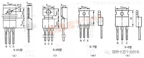
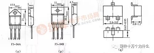
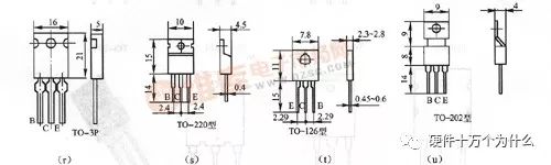
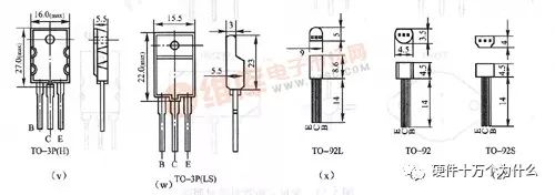
Figure 2 Transistor shape and size (continued)
The package comparison diagram of the common triode is shown in Figure 3.
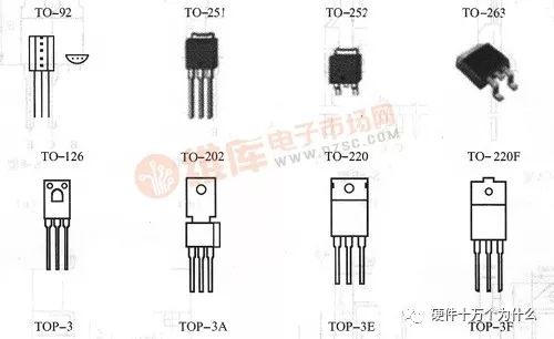
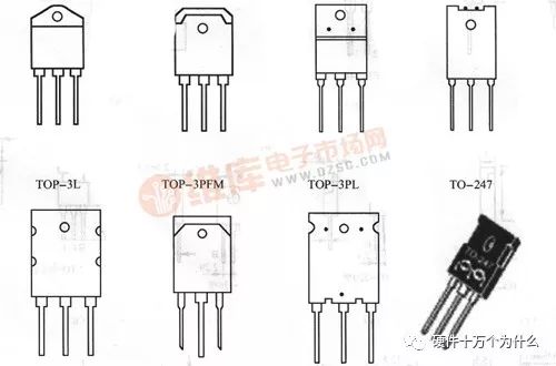
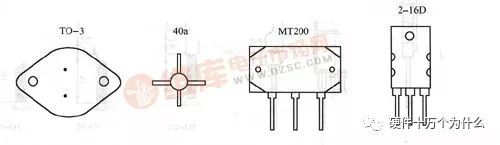
Figure 3 common triode package comparison chart
The physical diagram of the common triode package is shown in Figure 4.
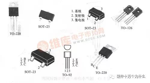
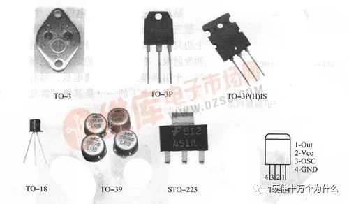
Figure 4 Common triode package physical map
2 pins
The arrangement of the triode pins has a certain regularity. For the domestic low-power metal package triode, the bottom view position is placed so that the three pins form the apex of the isosceles triangle, from left to right, E, B, C; the tube with the tube key, press from the tube key The hour hand direction is E, B, and C, and the pin identification diagram is shown in Figure 5(a). For the domestic medium and small power plastic sealing triode, the plane is facing outward, the semicircle is facing inward, and the three pins are placed upwards, then E, B, C are from left to right, and the pin identification diagram is shown in Fig. 5(b). ) shown.
At present, there are various types of crystal triodes on the market, and the arrangement of the pins is not the same. In the use of uncertain pins, columns of transistors, must be measured, or find the transistor manual, specify the special characteristics of the transistor and the corresponding technical parameters and information.
Today's more popular triodes 901 I ~ 9018 series are high-frequency small power tubes, except for 9012 and 9015 are PNP-type tubes, and the rest are NPN-type tubes.
Commonly used 9011 ~ 9018, C1815 series triode pin arrangement shown in Figure 6. The plane is facing yourself, the pins are facing down, and from left to right are E, C, and B.
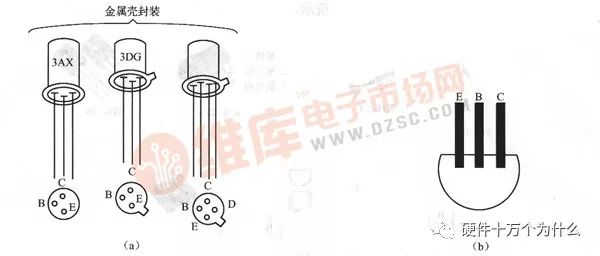
Figure 5 Domestic low-power transistor pin identification diagram
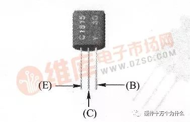
Figure 6 Common C1815 pin layout
The chip transistor has three electrodes and four electrodes. Generally, the three-electrode chip transistor has two sides viewed from the top, and only one leg on the upper side is a collector, and the lower two sides are a base and an emitter, respectively. In the four-electrode chip transistor, the larger one is the collector of the triode, the other two pins are the emitter, and the remaining one is the base. The outline of the common chip transistor pin is shown in Figure 7.
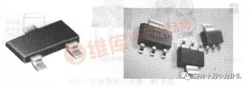
Figure 7 Common SMD Triode Pin Outline Drawing
Suspension Composite Insulator Polymer,High-voltage, Low-voltageMaterial,Composite Polymer
TAIZHOU HUADONG INSULATED MATERIAL CO.,LTD , https://www.thim-insulator.com