The Circuits from the Lab reference circuit is a tested reference design that helps accelerate design while simplifying system integration to help and solve today's analog, mixed-signal and RF design challenges.
Connection/reference deviceADF4351
35 MHz to 4400 MHz wideband frequency synthesizer with integrated VCO
ADL5801
10 MHz to 6 GHz wideband active mixer
AD8368
800 MHz, linear dB VGA, built-in AGC detector
ADL5902
50 MHz to 9 GHz, 65 dB TruPwrTM Detector
Frequency selection, RMS response, 90 dB dynamic range, 35 MHz to 4.4 GHz RF detector
Circuit evaluation boardADF4351 Evaluation Board (EVAL-ADF4351EB1Z)
ADL5801 Evaluation Board (ADL5801-EVALZ)
AD8368 Evaluation Board (AD8368-EVALZ)
ADL5902 Evaluation Board (ADL5902-EVALZ)
EPCOS B5249 SAW Filter Evaluation Board or equivalent
Circuit function and advantageThis circuit is a frequency-tunable radio frequency (RF) detector that provides a 90 dB detection range from 35 MHz to 4.4 GHz. Unlike independent detectors that do not distinguish between signals in the spectrum, this circuit can focus on a narrower frequency band to provide enhanced performance over a specified range. The detector circuit provides RMS response with excellent temperature and frequency stability and is attractive for applications that require precise frequency and selective RF power measurements. This circuit also suppresses unwanted blocking signals very well. Figure 1 shows the schematic diagram of the circuit.
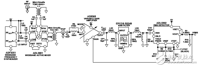
Figure 1. Frequency selective RF detector
Circuit descriptionThe detector circuit consists of an RMS detector, variable gain amplifier (VGA), SAW filter, mixer, and frequency synthesizer, providing a 90 dB detection range and excellent frequency/temperature stability. Figure 2 shows the transfer function of the detector circuit when the input power is scanned at 900 MHz. The best linearity is obtained with a 4-point calibration with calibration points of +13 dBm, −50 dBm, −65 dB, and −75 dBm. A 2-point calibration can also be used, but the linearity will decrease over the input power range.
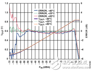
Figure 2. Transfer function of a frequency selective RF detector at different temperatures
Dynamic range enhancementThe ADL5902 detector used in the circuit itself provides a detection range of 65 dB and operates from 50 MHz to 9 GHz. The AD8368 VGA extends the upper and lower limits of the power range. The narrowband SAW filter between the VGA and the detector filters out the noise of the VGA and mixer, maximizing the lower sensitivity. Circuit Note CN-0340 illustrates this dynamic range extension mechanism in more detail. However, this range expansion limits the operation of the filter passband frequency range. The broadband frequency conversion network combined with the CN-0340 circuit allows the entire circuit to have frequency selection characteristics. In the circuit shown in Figure 1, the ADL5801 mixer is paired with the ADF4351 frequency synthesizer to convert the input signal from 35 MHz to 4.4 GHz to 140 MHz, the passband frequency of the SAW filter. Circuit Note CN-0239 illustrates the seamless wideband mixer and local oscillator interface used in this circuit.
The dynamic range of the circuit is further enhanced by optimizing the mixer bias level using the VSET pin of the mixer ADL5801. Typically, the ADL5801 mixer operates at a VSET level of 3.6 V, resulting in a higher mixer bias level and a correspondingly high IP3. However, this operating point can cause noise figure degradation, which limits input sensitivity. The mixer operates at a minimum VSET level of 2.0 V to improve the noise figure, but this affects the mixer's P1dB and limits the upper limit of the dynamic range. Therefore, the mixer needs to adopt an adaptive biasing mechanism to optimize the circuit detection range at both high and low power levels. By connecting the VSET pin to DETO (a pin routed to the internal power detector of the mixer), the device bias level can be adaptively set according to the signal conditions. With this feature, the mixer provides high linearity and compression for large RF signals while providing low noise figure for small RF signals. This feature improves the sensitivity of applications at lower input power levels while maintaining dynamic range at higher input power levels. Figure 3 shows the transfer function of the detector at different mixer bias levels.
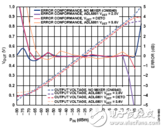
Figure 3. Performance comparison of ADL5801 mixers at different bias levels
Temperature stabilityFigure 2 shows the relationship between the temperature stability of the detector on the power spectrum and the RF input power. Accuracy over the temperature range is achieved with the temperature compensation feature of the ADL5902 RMS detector, which compensates for temperature drift introduced in the system. Any temperature change in the VGA and mixer gains will cause the overall drift of the circuit to drop by dB, which means that a 1 dB temperature drift of the mixer gain will reduce overall temperature stability by 1 dB. For the AD8368 VGA, Figure 5 in the AD8368 data sheet shows a temperature drift of approximately ±0.7 dB for its gain. Similarly, the mixer temperature drift is ±0.5 dB according to Figure 3 in the ADL5801 data sheet. Adjusting the voltage on the ADL5902 TADJ pin compensates for the total temperature drift of the detector, VGA, and mixer. The experiment found that a 0.6 V TADJ voltage provides the best temperature compensation for all RF input frequencies.
Frequency stabilityFigures 4 and 5 show the frequency flatness of the circuit. The circuit has a flatness of approximately 1 dB over the entire operating frequency range. Since the mixer downconverts the input signal to 140 MHz, the frequency flatness curve dominates the gain introduced by the mixer.
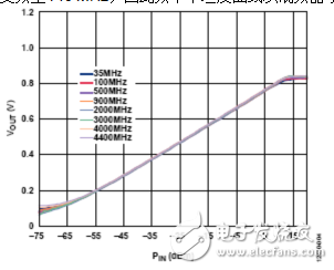
Figure 4. Output flatness versus input power at different frequencies
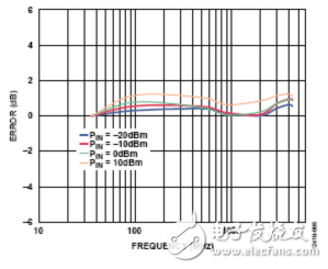
Figure 5. Error vs. frequency after 35 MHz calibration
Blocking signal suppressionFigure 6 shows the performance of the circuit at 900 MHz when there is a blocking signal of 960 MHz. The blocking signal is 60 MHz out of phase with the carrier signal because the passband rejection of the filter at this frequency is reduced (see Figure 7), which constitutes the most unfavorable test condition for the circuit. When the blocking signal input level is above −10 dBm, the blocking signal reduces the lower sensitivity of the circuit. However, for blocking signals up to +5 dBm, the circuit will maintain a dynamic range of 65 dB.
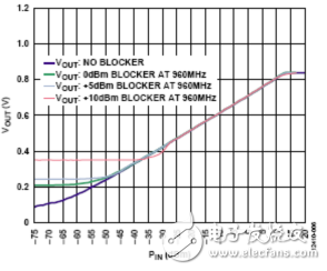
Figure 6. Output and input transfer functions at 900 MHz with a 960 MHz blocking signal
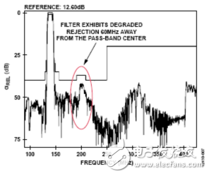
Figure 7. Transfer function of the EPCOS B5249 SAW filter
Common changesThe frequency range of the circuit can be extended to 6 GHz by replacing the frequency synthesizer ADF4351 with a wider bandwidth discrete phase-locked loop (PLL, such as the ADF4155 or ADF4156) and an external VCO. By changing the SAW filter, you can adjust the IF frequency, filter bandwidth, and insertion loss of the circuit. Increasing the bandwidth and insertion loss of the filter increases the noise level, which reduces the dynamic range of the system. The integrated output noise level of the mixer, VGA, and filter must be 6 dB to 10 dB below the nominal input sensitivity of the RMS detector. ADIsimRFTM can be used to calculate the integrated noise of the circuit front end (mixer, VGA, and filter). Connect the circuit to an analog-to-digital converter (ADC) such as the AD7091 or AD7466 to digitally convert the output voltage of the circuit. See Circuit Note CN-0178 for more information.
Circuit evaluation and testingThe circuit is implemented using the ADL5902 (ADL5902-EVALZ), AD8368 (AD8368-EVALZ), ADF4351 (EVAL-ADF4351EB1Z), ADL5801 (ADL5801-EVALZ) standard evaluation boards, and a filter evaluation board with an EPCOS B5249 SAW filter. Since all evaluation boards provide a 50 Ω interface, they are directly connected via a barrel SMA connector. Use the test clip to connect the signal from the ADL5902 detector output back to the AD8368 gain control input and connect the VSET and DET0 pins to configure the adaptive bias control of the ADL5801. The resistor divider required to reduce the ADL5902 detector output voltage is implemented by surface mount resistors on the R1 (3.83 kΩ) and R15 (1.5 kΩ) pads of the ADL5902 evaluation board. At 140 MHz, the TADJ voltage that optimizes the temperature stability of the circuit is set by the R9/R12 resistor divider, which takes the 2.3 V on-chip reference as an input. To set the TADJ voltage to the recommended 0.6 V level, change R9 to 850 Ω (R12 maintains the current value of 301 Ω).
Figure 8 shows a well-equipped application circuit, and Figure 9 shows a functional block diagram of the test setup.
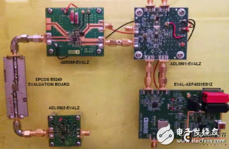
Figure 8. A well-assembled application circuit
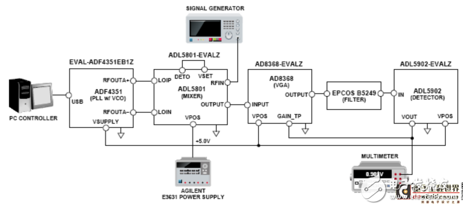
Figure 9. Circuit Evaluation Test Setup
Equipment requirementsA list of equipment used to evaluate the circuit is listed below.
• Windows® XP with USB port, Windows Vista (32-bit) or Windows 7 (32-bit) PC
• ADL5902-EVALZ, AD8368-EVALZ, EVAL-ADF4351EB1Z, and ADL5801-EVALZ evaluation boards
• EPCOS B5249 Evaluation Board
• An RF signal generator
• A digital multimeter
• One power supply
Use the ADF4351 control software to set the LO frequency required to downconvert the input signal to the 140 MHz IF. Then gradually increase the input power level and measure the RMS output voltage of the circuit to determine the transfer function and error consistency curve of the circuit.
To test the circuit's rejection of the blocking signal, a signal generator is used to simulate the blocking signal, and the main signal generator is used to simulate the target channel, and the two signals are used to drive the circuit. Then gradually increase the blocking signal level, observe the response of the circuit, and evaluate the circuit performance.
CN-0360 Design Support Package:
CN-0239 Circuit Note, Broadband 6 GHz Active Mixer with Seamless Local Oscillator Interface, Analog Devices.
The CN-0340 circuit notes a true RMS RF detector with a detection range of 95 dB, Analog Devices.
CN-0150 Circuit Note, Software Calibrated 1 MHz to 8 GHz, 70 dB RF Power Measurement System, Analog Devices.
CN-0178 Circuit Note, Software Calibrated 50 MHz to 9 GHz RF Power Measurement System, Analog Devices.
ADIsimRF design tool
ADIsimPLLTM Design Tool
UG-435 User Guide, Evaluation Board for the ADF4351 Fractional-N Frequency Division PLL Synthesizer.
UG-476 User Guide, PLL Software Installation Guide.
The MT-031 guide implements the grounding of the data converter and unlocks the mystery of "AGND" and "DGND", Analog Devices.
General-purpose rectifiers belong to the most widely used category of rectifiers, and their classification is relative to those with special functions, such as fast, high-frequency, and so on.
Our universal rectifiers are of original quality, complete models, high visibility, affordable prices, and fast shipping!
Rectifiers,General Purpose Rectifiers,Rectifier Diode,General Purpose Rectifier Diodes
Changzhou Changyuan Electronic Co., Ltd. , https://www.cydiode.com