There are several basic topologies in switching power supplies, such as buck topology circuits, boost topology circuits, and flyback switching power supplies. These topologies have both their similarities and their uniqueness. In general, experienced engineers can choose the appropriate topology according to their needs when designing. For beginners, how to choose the right topology is very difficult. Therefore, we need to master the basic features of the topology well. This is very necessary. This is also helpful for us to choose the right topology at design time, which can avoid wasting time because of improper topology selection.

Some topologies are suitable for off-line (grid-powered) AC/DC converters, some of which are suitable for low power output (<200W) and some are suitable for high power output; some are suitable for higher AC input voltage (>=220V AC), Some are suitable for lower AC input voltages; some have greater advantages at higher DC output voltages (>200V), and some have greater advantages at lower DC output voltages. For multi-level voltage output applications, the use of fewer devices or a good compromise between device count and reliability is a matter of choice for the topology. At the same time, the input/output ripple and noise requirements are also important factors in the selection of the topology. Certain topologies, because of their inherent limitations, require ancillary circuits or more complex circuits, making their characteristics very difficult to analyze in some applications.
Therefore, it is very important to properly choose the topology and to be familiar with the advantages and disadvantages of various basic topologies. The wrong choice can lead to poor performance of the power supply, and even waste design time and cost. Therefore, it is necessary to fully understand the basic characteristic parameters of different topologies.
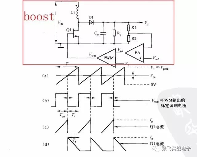
Figure 1 BOOST Circuit Topology and Waveforms
The Boost shown in Figure 1 raises the lower unregulated input voltage to a higher regulated output voltage. This circuit is called a boost regulator or a boost inductor converter.
When Q1 is turned off, the polarity of L1 is reversed; when Q1 is turned on, the energy stored in L1 is released to the output load through D1 at a higher voltage.
An inductor L1 is connected in series between Vdc and the switch Q1. When Q1 is turned on, current flows from the lower end of the inductor L1 to Q1. When Q1 is turned off, current is supplied from the lower end of the inductor L1 to the output capacitor C0 and the load through the rectifier diode D1.
Assuming that the output voltage and current have been established, the circuit has been operating stably. When the QI is on (TON), the diode reverses the bias and the linear rise of the current of L1 reaches the peak value Ip=Vdc TON /L1
Since the output current is completely provided by C0 during the conduction period of Q1, C0 should be selected to be large enough so that when the load is supplied to the load during the TON period, the voltage is minimized and the requirement is satisfied.
When Q1 turns off, because the inductor current cannot be mutated, the voltage polarity of L1 is reversed. The voltage of L1 is different from the same name.
positive. The terminal voltage of L1 of the same name is Vdc, and L1 is charged to C0 via D1, so that the voltage across C0 (pump-up voltage) is higher than Vdc. At this point, the inductor energy storage provides current to the load and supplements the charge that C0 loses when it supplies power to the load alone. Vdc also provides power to the load during the Q1 off period.
The adjustment of the output voltage is achieved by the negative feedback loop controlling Q1 conduction time. If the DC load current rises, then
The on-time will automatically increase to provide more energy for the load. If Vdc decreases and TON does not change, the peak current, that is, the energy stored in L1 will decrease, causing the output voltage to drop. However, the negative feedback loop will detect the voltage drop, and maintain the output voltage constant by increasing TON.
BOOST has two very different operating modes. These operating modes are related to the state of the inductor.
If the inductor current has dropped to zero at the end of one cycle, it operates in discontinuous mode. If the inductor current does not drop to zero at the end of one cycle, it operates in continuous mode.
When describing the switching topology, the output filter capacitor is generally not included in the topology. Therefore, the output current of the switching topology is not the DC current that is output to the load but the combined current that flows into the output capacitor and the load. The output capacitor and the load are connected in parallel.
Unlike the Buck topology, the input current to the Boost topology is continuous (with some ripple), and the output current is
Any mode of operation is not continuous. Therefore, the continuous mode and discontinuous mode are only for the current of the inductor.
As shown in Figure 1(d), the circuit operates in discontinuous mode when the D1 current drops to zero before the next Q1 pass.
If the current has not dropped to zero at the end of turn-off, the inductor current will not mutate and the current will rise when Q1 is turned on next time. The current on Q1 and D1 will have a typical step slope shape, as shown in Figure 2. As shown.

Figure 2 Current waveforms of boost topology Q1, D1, and L1 in continuous mode
The circuit operates in continuous mode at this point because the inductor current is always greater than zero during one duty cycle.
Assuming that the feedback loop can control the output voltage constant, when the R0 or Vdc decreases, the feedback loop will increase the Q1 cross-time Ton to keep the output voltage constant. When the load current increases, R0 or Vdc continues to decrease, then the Ton may increase, and the currents of Q1 and D1 do not drop to zero before the next turn-on, and the circuit enters the continuous operation mode at this time.
The error amplification that enables stable operation of the feedback loop in discontinuous mode does not necessarily stabilize the feedback loop in continuous mode and can cause oscillations. Theoretical analysis of the feedback loop states that there is a right half-plane zero for the transfer function of the boost circuit in the continuous operation mode, and the only way to stabilize the feedback loop with the right half-plane zero is to significantly reduce the bandwidth of the error amplifier.
In short, the inductor and D1 currents are zero for some time in a discontinuous mode of operation. That is, there is a small time gap during energy transfer (Q1 off and D1 on) and energy storage (Q1 on and D1 off). This time margin (dead zone) is very important for the operating characteristics of the power system and it does not exist in continuous operation mode.
It is very important to fully understand these two modes of work. Because in any switch topology with Boost functionality, it’s
The impact is very great. To better understand this point, we will analyze the response characteristics of the circuit when the load suddenly increases in the BOOST topology continuous operation mode.
Assume that a Boost circuit in a continuous operation mode has entered a stable operation state, the output voltage and load current are stable, and the inductor current is continuous. When the load current suddenly increases, the output voltage will have a decreasing trend. At this time, the control loop will increase the on-time of Q1 to increase the current of the inductor L1. However, after a few cycles, the current of the inductor L1 can increase very large (determined by the actual value of the inductor value, the input voltage, and the on-time of Q1).
It must be noted that the direct effect of the increase in on-time is to reduce the off-time because the period of one cycle is fixed. Since D1 is only turned on during Q1 turn-off (and the turn-on time is reduced), the average output current starts to decrease rather than increase. Therefore, when we try to increase the output current, this direct effect will reduce the output current, which needs to be gradually adjusted after several cycles of the increase of the inductor current.
Video Brochure
 |
Video Brochure,LCD Video Booklets,MP4 Greeting cards as the Multimedia Promotional Plan, have been widely
used in some occasings, such as graduations, birthday parties, weddings, opening veremonies, company intruction
and other commercial or industrial purposes.
· High resolution LCD screens use thin-film transistor technology for the ultimate display
· Crystal clear audio that is synced with your video
· Custom designed, printed and programmed for UP remium mailable package for Video PrintAd
Specifications:
· LCD SCREENS: 2.4″, 2.8",3.5″, 4.3″,5", 7.0″,10.1"
· MEMORY: 256MB~2G (15 – 60 Minute Video Playback)
· LIFE: 2-3 hours of continuous playback, 6-12 months standby (battery life)
· USB PORT: Usb access for recharging unit and uploading/modifying content
· BATTERIES: Internal Li-ion battery. Rechargable via USB. 15-30mins recharge time.
Options:
· Buttons for Multiple Video Activation
· On/Off Button
· On-Open Activation via a Sensor
· Volume Control
· Specialty Finishing (Spot UV, Embossing, Gold/Silver Foil, Pantones, Metallic Inks, more)
· Cover Materials: Card Stock, Board stock, Leather & Plastic
· AC Power Source Capable
· Continuous Run Cycle
· Motion Activation
· USB Cable
Video Brochure, Video Brochure Card, LCD Video Brochure
AST Industry Co.,LTD , https://www.astsoundchip.com