Current series negative feedback amplifier
As shown in Figure 8, it is a first-level common emitter amplifier, and R3 constitutes a current series negative feedback circuit.
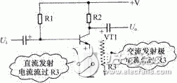
Figure 8 Current series negative feedback circuit
R3 is the VT1 emitter negative feedback resistor, R3 is connected in the emitter loop, and the emitter is the common input and output loop of this amplifier, so R3 is connected between the input and output of the amplifier, it is possible Form a negative feedback circuit.
1. Negative feedback circuit analysisAfter the VT1 emitter current flows through resistor R3, a voltage drop is generated across R3, which is the feedback signal voltage.
The negative feedback process analysis assumes that the VT1 base signal voltage increases at a certain moment, which leads to an increase in the VT1 base current, which increases the VT1 emitter signal current, and the emitter current flows through the resistor R3, causing the signal voltage drop on R3 to increase. That is, the VT1 emitter signal voltage increases, which causes the VT1 forward bias voltage (the circuit between the base and the emitter) to decrease, and the VT1 base current decreases, so this is a negative feedback process, and R3 constitutes Negative feedback circuit
The negative feedback signal voltage on resistor R3 is in series with the input signal, so this is a series negative feedback circuit.
[Negative feedback amount prompt]:
In this negative feedback circuit, if the magnitude of the VT1 emitter current is constant, the larger the negative feedback resistor R3 is, the larger the negative feedback signal voltage on R3 is, the larger the VT1 base current is reduced, that is, the negative feedback amount is increased. Larger, the smaller the gain of the amplifier, the opposite is the opposite. In the circuit, since both DC and AC current flow through the negative feedback resistor R3, R3 has a negative feedback effect on both DC and AC.
2. Emitter negative feedback resistor circuit with bypass capacitorThe triode emitter resistor constitutes a current series negative feedback circuit. This circuit has various deformation circuits depending on whether or not the emitter bypass capacitor is connected and the capacitance capacity is different.
As shown in Figure 4-9, the emitter negative feedback resistor circuit with bypass capacitor is also the primary audio amplifier.
A larger capacity bypass capacitor C1 is connected in parallel with the emitter negative feedback resistor R1. The capacitive reactance is much smaller than the resistance of the emitter resistor R1, and the AC signal current output by the VT1 emitter passes through C1 to the ground. Can't flow through R1.
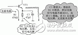
Figure 4-9 Emitter negative feedback resistor circuit with bypass capacitor
R1 is the emitter negative feedback resistor. When no C1 is connected, the DC current flowing from the VT1 emitter and the AC signal current flow through R1 to the ground. R1 has a negative feedback effect on both DC and AC. After adding C1, R1 only has DC negative feedback, because the AC signal current does not flow through R1, so R1 has no negative feedback effect on the AC signal.
F, for the audio amplifier, the capacitance is very large, it has a small capacitive reactance for all frequency audio signals, so it can pass audio signals of all frequencies. m can be seen from the figure, the capacity of C1 is 47
The method for judging what kind of signal negative feedback exists in the emitter resistance is:
What kind of current flows through the emitter resistance, what kind of signal voltage exists, what kind of negative feedback exists, so as long as the analysis of what kind of current flows through the emitter resistance.
3. Partial emitter resistance plus bypass capacitor circuitAs shown in Figure 4-10, the circuit of the partial emitter resistor plus the bypass capacitor is shown. In the emitter circuit, the emitter resistance is sometimes divided into two series in order to obtain proper DC and AC negative feedback.
R1 and R2 are connected in series as the total emitter resistance of VT1, and are divided into R1 and R2 series circuits in order to facilitate the addition of different amounts of DC and AC negative feedback.
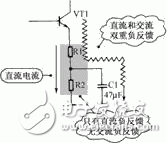
Figure 4-10 Partial emitter resistance plus bypass capacitor circuit
DC current loop DC current flows through R1 and R2, so both resistors have DC negative feedback
AC current loop VT1 emitter AC current through R1 and C1 to ground, no flow through R2, so only R1 has AC negative feedback
The purpose of this emitter resistance design is to obtain greater DC negative feedback while reducing AC negative feedback, because the AC negative feedback amount is too large, the amplifier's gain will drop too much.
[Analysis Tips]:
For this multiple emitter resistor series circuit, the key to analyze which resistor is DC or AC negative feedback is to see what current flows through the resistor. If only DC current flows through the resistor, there is only DC negative feedback. If an alternating current flows through the resistor in addition to the direct current, the resistor has double negative feedback of alternating current and direct current.
4. Emitter negative feedback resistor circuit with high frequency bypass capacitorF). mF, so VT1 constitutes an audio amplifier, and a smaller capacity bypass capacitor C2 is connected to the VT1 emitter resistor (1m is an emitter negative feedback resistor circuit with a high-frequency bypass capacitor as shown in Figure 4-11. Input coupling capacitor C1 capacity is 10
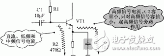
Figure 4-11 Emitter negative feedback resistor circuit with high frequency bypass capacitor
The low frequency and intermediate frequency signals in the DC and audio signals all have a negative feedback effect F). The capacitive reactance of the low frequency and intermediate frequency signals in the audio signal is much larger than the resistance of the resistor R2, so that C2 is equivalent to an open state, and the audio signal is in this case. The low frequency and intermediate frequency signals flow through the resistor R2 because of the large capacitive reactance of C2, so R2 has a negative feedback effect on the low frequency and intermediate frequency signals in the DC and audio signals. m for audio amplifiers, because C2 capacity is relatively small (1
High frequency bypass capacitor. For the high frequency signal in the audio signal, the C2 capacitive reactance is relatively small, because the frequency of the high frequency signal is high, so the capacitive reactance is small. C2 constitutes the high-frequency signal current path of the VT1 emitter output, which acts as a high-frequency bypass, so R2 has no high-frequency negative feedback. Thus, the negative feedback amount of the amplifier to the high frequency signal is small, and the amplification factor of the high frequency signal is larger than the amplification factor of the low frequency and intermediate frequency signals. Such a circuit is called a high frequency compensation circuit. A capacitor such as C2 that allows only high-frequency signals in an audio signal to flow is called a high-frequency bypass capacitor.
F, but the capacitive reactance is already very small, much smaller than the emitter negative feedback resistor R2, and all high frequency signals flow through C2 to the ground. After adding C2, R2 has no negative feedback of high frequency signal, and only DC negative feedback exists. m If the VT1 tube is composed of a high-frequency amplifier (the coupling capacitance of the input terminal in the circuit is reduced by several hundred picofarads), the operating frequency of the high-frequency amplifier is much higher than the frequency of the audio signal, because the frequency of the signal itself is high, although the C2 capacity is high. Only 1
[Analysis Tips]:
Capacitor C2 of F has a different role in the amplifiers of different operating frequencies. For audio signals, C2 bypasses only the high frequency signals in the audio signal; for high frequency amplifiers, it bypasses all high frequency signals. m through the analysis of this circuit, we can not only understand what type of amplifier is in the circuit analysis, understand the characteristics of the components in the circuit, and sometimes need to know the size of the component nominal value, otherwise the circuit analysis is not accurate, for example The same in the circuit is 1
5. Emitter resistor circuit with different capacity bypass capacitorsAs shown in Figure 4-12, two different capacity bypass capacitors are connected to the emitter resistor circuit. In the circuit, VT1 constitutes an audio amplifier circuit, which has two emitter resistors R2 and R3 connected in series, and two emitter bypass capacitors C2 and C3 of different capacities. Due to the small capacity of C2, the capacitive reactance of the high frequency signal in the audio signal is small, and the capacitive reactance to the intermediate frequency and low frequency signals is large.
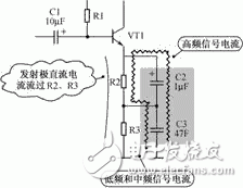
Figure 4-12 Emitter resistor circuit with two different capacity bypass capacitors
The negative feedback resistor R2 has low frequency and intermediate frequency signal currents in DC and audio signals, so there are DC, low frequency and intermediate frequency negative feedback. C2 only allows high frequency signals in the audio signal to flow.
The negative feedback resistor R3 has a DC current, so there is only DC negative feedback, and C3 allows the low, medium and high frequency signals in the audio signal to pass.
6. Judging current negative feedback circuit methodThe current negative feedback circuit is judged as follows: As shown in Figure 4-13, if the output of the amplifier is shorted to ground, the negative feedback in the amplifier still exists, then the current is negative feedback circuit, otherwise it is not the current negative feedback. Circuit.
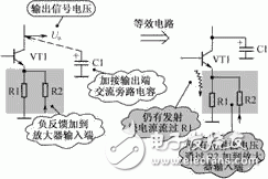
Figure 4-13 Schematic diagram of the method for judging the current negative feedback circuit
7. Series negative feedback circuit judgment methodWhen the negative feedback signal and the input signal are added to the amplifier at different terminals (the base and emitter of the triode, respectively), this is a series negative feedback circuit, as shown in Figure 4-14.
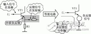
Figure 4-14 Schematic diagram of the method for judging the series negative feedback circuit
24 hours mechanical Timer
Instant indicator
Min.setting time:15 minutes. Max.setting timer:24 hours
With hand switch,can be switched to operating and
setting at any time
Instructions:
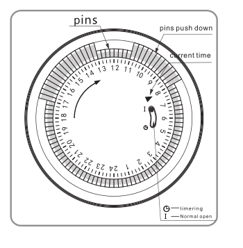
1. Set program: 1 pin is equivalent to 15 minutes. Determine desired start time and push down pins until desired
off time.
For instance, if you want electrical devices to work from 8:00am to 11:00am and from 13:00pm to 17:00pm, you
just need to put down allthe pins between the three period time.
2. Set the current time: Turning the dial clockwise until the arrow pointing to
current time.
For example,if now it is 8:00 am, please turn the dial and make sure the
arrow point to 8. (See the picture.)
3. Plug the electrical device directly into the timer. Make sure the electrical
device is power-on.
4. Plug the timer into electrical outlet and the electrical device will be work
according to the setting program.
Note: = Normal Ope n = Timing
Make sure the switch on the Timing position. If it
is on the [Normal Open" mode, the electrical device is
always power-on and the timer function no work.
Specifications:
|
Rated Voltage, Current and Power |
As shown on the label |
|
Time Setting Range |
15minutes24hours |
|
Working Temperature |
-10℃?+55℃ |
|
Operation |
Clockwise |
|
Insulation Resistance |
>100M |
|
Inherent Loss |
≤1W |
Application:
1. To enable high-power electric appliances to run automatically at off-peak time if there is different electricity
price according to different periods of time in some areas.
2. To use for electric appliances which need time control, such as water heaters, air conditioners, drinking
fountains, rice cookers, advertising lights and so on.
3. To control the charging time. For example, battery of electric bikes or mobile phones, storage batteries, etc.
4. Occasions which need switch on/off frequently, like interval spray irrigation for flowersand lawn, cyclical
adding oxygen to fish jar, fountains and so on.
5. Home safety precautions and lighting.
Caution:
1.D o not exceed the maximum ratings of the timer.
2.M ust reset the current time after power failure.
3.D o not plug the timer directly into the working electrical appliances.
4.U nless changing the setting, keep the program same every day.
5.D o not disassemble timer by yourself. Professionals service are needed for maintenance.
6.T his item is only for indoor use.
Mechanical Timer, mechanical timer socket, 24hr mechanical timer, mechanical timer plug, mechanical timer adaptor
NINGBO COWELL ELECTRONICS & TECHNOLOGY CO., LTD , https://www.cowellsocket.com