The reality of physical processes makes it impossible to obtain an ideal op amp with perfect precision, zero noise, infinite open loop gain, slew rate, and gain bandwidth product. However, we expect that generations of successive amplifiers will be better than previous generation amplifiers. So what happens to the next step of a low 1/f noise op amp?
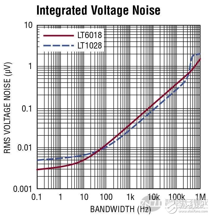
Back in 1985, ADI's George Erdi designed the LT1028. After more than 30 years, the device is still the lowest voltage and noise op amp in the market at low frequencies, with an input voltage noise density of 0.85nV/√Hz at 1kHz. The input voltage noise at 0.1 Hz to 10 Hz is 35nVP-P. Until this year, a new amplifier, the LT6018, challenged the position of the LT1028. The LT6018's 0.1Hz to 10Hz input voltage noise is 30nVP-P and has a 1Hz 1/f corner frequency, but its wideband noise is 1.2nV/√Hz. As a result, the LT6018 is a lower noise option for lower frequency applications, while the LT1028 provides better performance for many broadband applications, as shown in Figure 1.

Figure 1: LT1028 and LT6018 integrated voltage noise
Noisy noise is distressing
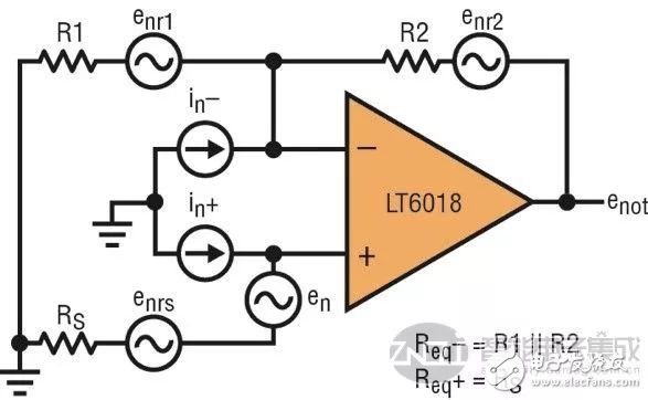
However, designing a low noise circuit is much more complicated than selecting an amplifier with the lowest voltage noise density (en) for a given frequency band. As shown in Figure 2, other noise sources begin to function, and the incoherent noise sources are combined in a sum of square roots.

Figure 2: Op amp circuit noise source
First, consider the resistor as a source of noise. The resistor is inherently noise proportional to the square root of the resistance value. At a temperature of 300K, the voltage noise density of any resistor is en = 0.13 √ R nV / √ Hz. This noise can also be considered as a Norton equivalent current noise: in = en / R = 0.13 / √ R nA / √ Hz. Therefore, the resistor has a noise power of 17 zeptoWatts. A good op amp will have a noise power below this value. For example, the noise power of the LT6018 (measured at 1kHz) is approximately 1 zeptoWatt.
In the op amp circuit of Figure 2, the source resistor, gain resistor, and feedback resistor (RS, R1, and R2, respectively) are factors that generate circuit noise. When calculating noise, the “√Hz†used in the voltage noise density can cause confusion. However, together they are noise power, not noise voltage. Therefore, to calculate the integrated voltage noise of a resistor or op amp, multiply the voltage noise density by the square root of the Hertzian number in the band. For example, a 100Ω resistor has 1.3μV RMS of noise (0.13nV/√Ω * √100Ω * √1,000,000Hz) in a 1MHz bandwidth. For circuits that use a first-order filter instead of a brick-wall filter, the bandwidth is multiplied by 1.57 to capture noise over a higher bandwidth. To express noise as “peak to peak†instead of “RMS valueâ€, multiply by a factor of 6 (instead of 2.8 for sinusoidal signals). With these factors in mind, the noise of this 100Ω resistor is close to 9.8μVP-P when using a simple 1MHz low-pass filter.
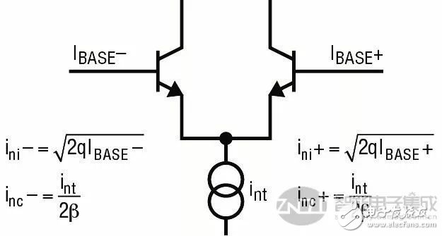
In addition, the op amp has input current noise (in- and in+) caused by current flowing into and out of each input. These are multiplied by the resistance they flow into (the parallel resistance of R1 and R2 for in-, and the parallel resistance of R1 to RS for in+), which produces voltage noise with the "magic" of Ohm's law. Looking inside the amplifier (Figure 3), the current noise is made up of multiple noise sources.

Figure 3: Coherent and incoherent noise sources in an op amp differential pair
In terms of broadband noise, both input transistors have point noise (ini- and ini+) associated with their base, which are irrelevant. The noise (int) from the current source at the end of the input pair also produces coherent noise (int/2β in each input) divided between the two inputs. If the resistances carried on the two inputs are equal, the coherent voltage noise on each input is also equal and canceled (according to the amplifier's common mode rejection capability), thus leaving mainly incoherent noise. This is listed as balanced current noise in the product manual. If the resistances on the two inputs are greatly mismatched, the coherent and incoherent noise components remain and the voltage noise is summed by the sum of the square roots. This is listed as unbalanced noise current in some product manuals.
The voltage noise of the LT1028 and LT6018 is lower than a 100Ω resistor (1.3nV/√Hz at room temperature), so in high-source applications, the op amp's voltage noise is usually not a limiting factor in the circuit. With much lower source resistance, the amplifier's voltage noise will begin to dominate. When the source resistance is very high, the amplifier's current noise dominates, while for medium-level source resistance, the resistor's Johnson noise has a decisive influence (for those that do not have excessively high noise power) Design an op amp). The resistance that balances the amplifier's current noise and voltage noise (so the two are not dominant) is equal to the amplifier's voltage noise divided by its current noise. Since the voltage and current noise vary with frequency, so is the midpoint resistance. For an unbalanced power supply, the midpoint resistance of the LT6018 is approximately 86Ω at 10Hz and approximately 320Ω at 10kHz.
Minimize circuit noise
So what steps does the design engineer take to minimize noise? For processing voltage signals, reducing the equivalent resistance below the midpoint resistance of the amplifier is a good starting point. For many applications, the source resistance is fixed by the previous circuit level (usually a sensor). Small gain and feedback resistors can be selected. However, since the feedback resistor forms part of the op amp load, there are limitations due to the output drive capability of the amplifier and the acceptable amount of heat and power dissipation. In addition to the resistance carried by the input, the frequency should also be considered. The total noise includes the noise density that is integrated over the entire frequency range. It is important to filter the noise at frequencies above (and perhaps below) the signal bandwidth.
In a transimpedance application where the input of the amplifier is a current, a different strategy is required. In this case, the Johnson noise of the feedback resistor is increased by a square root factor of its resistance value, but at the same time the increase in signal gain is linear with the resistance value. Thus, the optimal SNR is achieved by the voltage capability of the op amp or the maximum resistance allowed by the current noise. For an interesting example, see the application circuit on page 26 of the LTC6090 Product Manual.
Noise and other headaches
Noise is only a source of error and should be considered in the context of other sources of error. The input offset voltage (voltage mismatch on the op amp input) can be considered as DC noise. Although its effect can be significantly suppressed by implementing a one-time system calibration, the offset voltage changes with temperature fluctuations and time due to mechanical stress changes. In addition, it varies with input level (CMRR) and power supply (PSRR). Real-time system calibration designed to eliminate drift caused by these variables quickly becomes both expensive and impractical. For harsh environmental applications where temperature fluctuates significantly, measurement uncertainty due to offset voltage and drift produces a dominant effect than noise. For example, an op amp with a 5μV/°C temperature drift performance will experience a 625μV input reference offset over the -40°C to 85°C temperature range due to temperature drift alone. In contrast, noise of a few hundred nanovolts (nV) is irrelevant. The LT6018 has excellent drift performance of 0.5μV/°C and a maximum offset of 80μV (from -40°C to 85°C). For better performance, consider the recently introduced LTC2057 auto-zero amplifier, which has a maximum offset voltage of less than 7μV over the -40°C to 125°C temperature range. Its broadband noise is 11nV/√Hz, and its DC to 10Hz noise is 200nVP-P. Although this noise is higher than the LT6018, the LTC2057 is sometimes a better choice for low frequency applications due to its excellent input offset drift over temperature. It is also worth noting that the LTC2057 has much lower current noise than the LT6018 due to its low bias current. Another benefit of the LTC2057 low input bias current is that it has a very low clock feedthrough compared to many other zero-drift amplifiers. Some of these other zero-drift amplifiers generate large voltage-noise spurious signals when the source impedance is high.
In such high-precision circuits, the thermocouple effect must also be discreetly minimized, and this effect occurs in any situation where a heterogeneous metal junction exists. Even the junction of two copper conductors from different manufacturers produces a thermoelectric potential of 200nV/°C, which is more than 13 times higher than the worst drift of the LTC2057. In these low drift circuits, it is important to use the correct PCB layout method to match or minimize the number of nodes in the amplifier input path, to keep the input and matching nodes close together, and to avoid thermal gradients.
in conclusion
Noise is a fundamental physical limitation. In order to minimize the adverse effects of processing the sensor signals, care must be taken in selecting the appropriate op amp, minimizing and matching the input resistance, and implementing the physical layout of the design.
The cat7 Lan Cable are an eight-core Shield wire. Each pair has a Shield layer (commonly called a Foil Shield), and then a Shield layer (commonly called a Braided screen Shield) outside the eight cores, with the same connection as the RJ-45.The highest transmission frequency of the CAT7 Ethernet Cable S/FTP is 600MHz, and the transmission frequency of the CAT7 Network Cable is 1000MHz.
There are a number of significant differences between the six and seven cabling systems, the most obvious of which is bandwidth.The CAT6 cable of channels provide a comprehensive attenuation to crosspoint ratio of at least 200MHZ and an overall bandwidth of 250MHZ. CAT7 of systems can provide at least 500MHZ of comprehensive attenuation to crosspoking ratio and 600MHZ of overall bandwidth.
The proliferation of broadband applications has created a need for more bandwidth.For example, a typical CAT7 channel can provide a bandwidth of 862MHZ for the transmission of video signals, analog audio signals on another pair, and high-speed LAN information on a third or fourth pair.
Another difference between the CAT6 patch cable and cat7 patch cable systems is their structure.The six types of wiring systems can use either UTP or STP.The seven types of systems are based only on shielded cables.In the cat7 network cables, each pair has a shield layer, and four pairs of wires together have a common shield layer.In terms of physical structure, the additional shielding layer makes the CAT7 Ethernet Cable have a larger diameter.
Another important difference is its ability to connect hardware. The parameters of the cat7 patch cable of systems require that all pairs of wires provide at least 60DB of integrated proximal winding at 600MHZ.The cat6 systems only require 43dB at 100MHZ and 46dB at 250MHZ for the cat6 patch cable.

Cat 7 Ethernet Cord,Cat7 Lan Cable,Cat 7 Ethernet Cable,Cat 7 Network Card
Shenzhen Kingwire Electronics Co., Ltd. , https://www.kingwires.com