First, the performance characteristics of EM78P447S microcontroller
The EM78 series of microcontrollers are 8-bit microcontrollers fabricated in a low power, high speed CMOS process. This lecture will take the EM78P447S microcontroller with OTP program memory (read-only memory that can be programmed once) as an example to describe the functional characteristics, internal structure, program memory, data memory, interrupt system, input/output port, Timer/counter, watchdog timer, clock oscillator, and reset system.
The performance characteristics of the EM78P447S MCU are summarized as follows:
1. Wide operating frequency range: DC ~ 20MHz.
2. Wide operating voltage range: 2.2 to 5.5V.
3. Operating temperature range: 0 ~ 70 ° C.
4. Low power consumption: less than 2.2mA at 5V/4M operating conditions, 30μA at 3V/32K, and 1μA in sleep mode.
5. It comes with a 4K x 13-bit on-chip OTP-ROM program memory.
6. With program encryption measures, you can protect programs from being illegally read.
7. It has 148×8-bit on-chip data registers (ie, static memory, SRAM).
8. It has three bidirectional I/O (input/output) ports, each of which can be programmed independently.
9. It has an 8-bit wide timer, counter, its signal source and trigger edge are all programmable, and an interrupt is generated when it overflows.
10. There are two power saving modes (sleep mode) to help extend the life of the power supply battery.
11. Free running watchdog timer.
12. Has 2 hardware interrupt sources: external pin trigger interrupt; timer, counter overflow interrupt.
13. 10 pins with wake-up function for input status change (can be used to wake up the microcontroller in sleep mode).
14.10 internal pull-up function programmable I/O pins. 15.2 Internal Open-Drain Function Programmable I/O Pins.
16.2 I/O pins with R-OPTION function (this function will be explained later).
17. All instructions in the command system are of uniform length, that is, all 13-bit long instruction words. In some other microcontrollers (such as the common 8051 series); the instruction system has single-byte, double-byte and three-byte instructions, and the instruction length is not uniform. Take a total of 5 levels of hardware stack structure to facilitate the operation of the stack.
19. Adopting the Reduced Instruction Set (RISC) technology, its instruction system has only 58 instructions, which is easy to learn and use.
20. The addressing method is simple, easy to master, and easy for beginners to get started.
21. The peripheral circuit is simple. EM78P447S microcontroller integrates power-on reset, I/O pin pull-up, open-drain, watchdog and other functional circuits, which can minimize or eliminate external circuits, and facilitate the realization of "single-chip" application of single-chip microcomputer system. .
twenty two. Each instruction cycle contains only 2 clock cycles internally.
23.99.9% of the instructions are single instruction cycles (ie, they can be run within one instruction cycle).
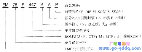
twenty four. Available in two package models: EM78P447SA and EM78P447SB are available in 28-pin and 32-pin packages.
25. Available in 2 package styles: dual in-line DIP and surface mount SOIC.
With regard to some of the terminology mentioned above, further explanations will be made later in the context of where they are involved.
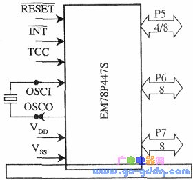
Second, the pin J of the EM78P447S can
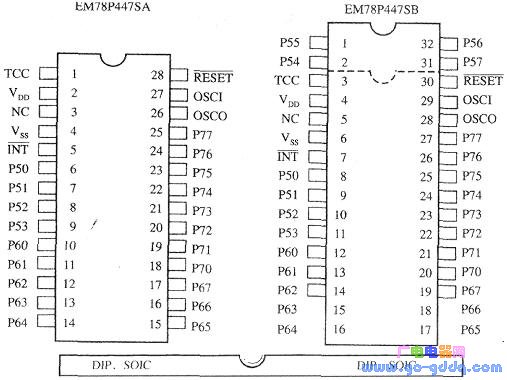
The pinout sequence and logic symbols of the EM78P447S are shown in the above figure and the following figure, respectively. The function of each pin is shown in Table 1. As can be seen from Figure 1, in fact, the A type is obtained after reducing the four pins P54 to P57 on the basis of BJ. The other pins are fully compatible, which is very convenient in the product development process, from the A type to Type B extension. The EM78P447S has 28 or 32 pins, and the function of each pin is very different. However, if you classify the pin functions, you can divide all the pins into 4 categories:
â— Control class: reverse of RESET, reverse of TCC and INT;
â— Clock class: OSCI and OSCO;
â— Power class: VDD and Vss;
â— Port class: There are 3 input/output (I/O) ports for P5, P6 and P7. In this way, the logical symbols shown in Figure 2 appear to be more concise than Figure 1.
Third, the internal structure of EM78P447S
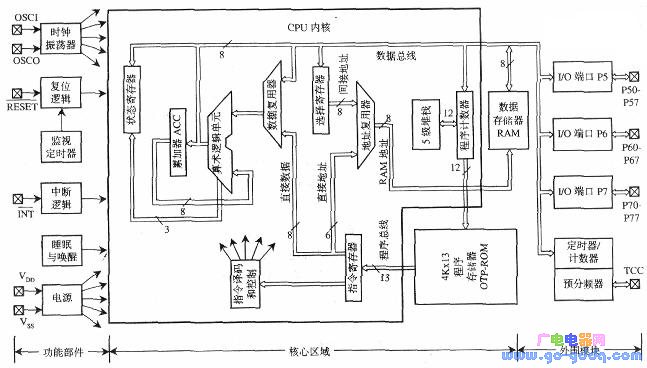
The functional block diagram of the internal structure of EM78P447S is shown in the figure above: For a single chip microcomputer, the most important part is the "CPU core", which is extended to the periphery, and the program memory and data memory which are usually configured by some single chip chips are included. The "core area" of the microcontroller chip; and then to the peripheral extension, the first is the "functional circuit components" of the microcontroller, and finally some "peripheral modules."
For any single-chip microcomputer in the EM78 series, its "core area" is unique and indispensable. "Functional circuit components" are also universally configured, and the types and quantities of "peripheral modules" can be completely The manufacturer flexibly adapts and increases or decreases according to the design goals and uses of the microcontroller. Below we first introduce the unit circuits and their functions in the core area of ​​EM78P447S comprehensively and briefly, and let the readers establish a macro understanding of the core hardware of the MCU as soon as possible. For the various functional components and peripheral modules around, because the functions are relatively independent and complex, they are ready to be explained in the following chapters.
1. Cell circuit in core area and its function
(1) Data bus: 8 bits wide, as a dedicated channel for data transmission. Link each peripheral module and the core part of the PC, FSR, STATUS, WDT, ALU, RAM and other functional components:
(2) Program bus: 13 bits wide, as a high speed channel for extracting program instructions. Full-time implementation of each instruction from the program memory to the instruction register in a fast and timely manner; (3) program memory (ROM): store the user program pre-programmed by the user and some fixed data; (4) program counter (PC) : Generate and provide the 12-bit address code required to extract instructions from the program memory unit. Each time an instruction is executed, the address code is automatically incremented by one; (5) the instruction register: temporarily stores the instruction fetched from the program memory, and presses the instruction Different fields are decomposed into two parts: the opcode (which directs the CPU to perform operations such as adding, subtracting, etc.) and the operand (indicating the data itself participating in the operation or the address of the data), which are sent to different destinations; 6) Instruction Decoding and Control Logic: This part of the circuit consists of a large and complex decoding matrix that "interprets" the opcode portion of an instruction in the instruction system into a series of micro-operation control signals to control all Each functional circuit participating in the operation performs coordinated operation, and finally implements the specific operation specified by the instruction; (7) Arithmetic Logic Unit (ALU): is a very important The meta-circuit realizes arithmetic operations such as addition, subtraction, multiplication, and division, and logical operations such as left shift, right shift, set, clear, bit test, etc.; (8) Accumulator (ACC or A): is one of the most important Using the most frequent central registers, many instructions operate as a transit point for data. For example, temporarily store a data that is ready to participate in an operation, or a result of a temporary operation. In other words, ACC is the starting point of the original data before the operation, and ACC is the landing result of the result data after the operation; (9) Status register (STATUS): mainly to record some arithmetic features of the operation result in the ALU, such as whether Generate carry, borrow, all zero, etc.; (10) Data Memory (RAM): used to store the intermediate data generated by the CPU during the execution of the program. Ordinary RAM memory can only achieve data writing and reading, and some memory cells of RAM memory in EM78 are much more powerful. In addition to common memory functions, they can also be shifted, set, and cleared. Bit, bit test, etc. A series of complex operations that can only be completed by "registers"; (11) Data multiplexer: It selects and passes another source operand that participates in the operation, either from the data memory RAM or directly From the instruction code; (12) address multiplexer: access (that is, read or write) the address required for the data memory is selected and passed by the address multiplexer, the address can be derived from the "indirect addressing register" RSR" can also be directly derived from the instruction code. The address from the RSR is called the indirect address, the address from the instruction code is called the direct address, and (13) the indirect addressing register RSR: the indirect address for the data memory RAM. Put the address of a working register that you plan to access in advance into the RSR register; (14) Hardware Stack: Save the program breakpoint address. During the execution of the program, it is sometimes necessary to jump to the "subprogram". Before entering the subroutine, the address of the main program breakpoint must be saved so that the breakpoint address can be restored after the subroutine is executed. Allow the main program to continue execution.
| Pin name | Types of | The main function | |
| RESET | I | Manual reset signal input. Schmitt trigger input, the microcontroller resets when the pin is held low. When not connected to other circuits, connect this pin to VDD. | |
| TCC | I | Timer/counter input pin, Schmitt trigger input, ground or Vcc when the pin is not in use | |
| INT | I/O | External interrupt input pin, falling edge trigger interrupt | |
| OSCI | I | The input pin of the crystal oscillator. Provide clock pulse signal for single chip operation | |
| Osc0 | I/O | The output pin of the body oscillator is usually connected to a crystal oscillator between OSCI and OSCO. | |
| VDD | - | Positive power supply | |
| Vss | - | Negative power supply or ground | |
| P50~P53 | I/O | P50 to P53 are low 4-bit bidirectional I/O ports. P5 only uses these 4 pins in the EM78447A | |
| P54~P57 | I/O | P54 to P57 are high 4-bit bidirectional I/O ports. P5 is an 8-bit bidirectional I/O port in the EM78447B | |
| P60~P67 | I/O | P60~P67 are bidirectional I/O terminals L] | |
| P70~P77 | I/O | P70 to P77 are bidirectional I/O ports | |
| NC | Not connected, not used | ||
| Note: In addition to the main functions, some pins have additional functions, which will be detailed when they are used. | |||
2. Features and their functions
It is necessary to briefly describe several features below:
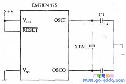
(1) Clock oscillator: It is the time base generator that generates the clock pulse signals required for the operation of each functional circuit inside the microcontroller chip. One of the most common circuit connection methods is to connect a crystal oscillator XTAL and two capacitors C1 and C2 to ground between the two pins of OSCI and OSCO, as shown in the figure above, and form a square together with the on-chip circuit. Wave oscillator circuit. Its operating frequency depends on the natural frequency of XTAL. (2) Reset logic: When the MCU chip is initially powered up and the power supply VDD rises to a voltage value suitable for the chip operation, or when a low-level reset signal is artificially sent from the external pin RESET, under the control of the reset logic The microcontroller performs a reliable reset and then executes the program from the beginning. The simplest way to connect a circuit is to connect the pin directly to the positive terminal of the power supply, as shown in Figure 4. (3) Power supply circuit: This circuit is responsible for distributing the power supply voltage applied between the VDD and VSS pins to various functional circuits within the microcontroller chip. As long as the power supply voltage does not exceed the range of 2.2 to 5.5V, the microcontroller can be guaranteed to work normally.
(4) Watchdog timer (commonly known as watchdog WDT): The watchdog only works when it is out of the normal track and enters a crash or chaos state during the execution of the program. It forces the microcontroller to reset to make it Execute the program from the beginning and return to normal working condition. In fact, the WDT is an up-counter with its own clock generator. Once an overflow occurs, the microcontroller is reset. It preempts the same divider with the timer/counter TCC module.
(5) Interrupt logic: The interrupt function is designed to enhance the ability of the microcontroller to handle various emergencies. When the MCU system is executing the program, some special conditions (such as timing time to wait) occur. At this time, the MCU needs to temporarily stop the currently executing main program, and then go to execute the subroutine that handles the special case. After the subroutine is executed, Going back to the breakpoint of the main program to execute, this forms an interrupt process. The interrupt process caused by various peripheral modules or functional components is managed by the interrupt logic.
(6) Sleep and wake-up logic: In order to reduce the power consumption of the microcontroller in standby state, it is an effective method to put it into sleep state. Once the full-function operation of the MCU is required, the MCU will wake up from the sleep state and enter the normal processing state. This circuit logic is required for the management of the sleep and wake-up process.
For the watchdog timer, interrupt logic, and sleep and wake-up logic, there are special sections that follow in detail with application examples.
3. Peripheral modules and their functions
For the EM78P447S microcontroller, two types of four peripheral modules are configured on-chip:
(1) Input, output port modules P5, P6 and P7: Both contain 8 port pins that can independently set the I/O direction. The two port modules have similar circuit structures. Its main function is to exchange information with external circuits.
(2) Timer/Counter TCC Module: This module is mainly used to implement timing or count external events. It grabs the same divider as the watchdog WDT.
Aluminum Electrolytic Capacitors/ Ceramic Capacitors
Aluminum Electrolytic Capacitors/ Ceramic Capacitors
Aluminum Electrolytic Capacitors,Electrolytic capacitor,Ceramic Capacitor
YANGZHOU POSITIONING TECH CO., LTD. , https://www.cndingweitech.com