As a relatively new technology, gallium nitride (GaN) adopts some technologies and ideas that are different from other semiconductor technologies. For newcomers to model-based GaN power amplifier (PA) design, after learning the basic concepts of nonlinear GaN models (how can nonlinear models help with GaN PA design?), understand the IV curve (also known as current-voltage characteristics) Curve) is a good starting point. This article explores the importance of IV curves and how their representation in nonlinear GaN models (such as those in the Modelithics Qorvo GaN library) can help you complete the design process more accurately and efficiently.
What is the pitch?
You can think of the IV curve as a football field (sometimes called "pitch"), whose limits determine the boundary of the microwave signal, as shown in the following figure. In short, once the boundary is touched, signal clipping occurs, which causes compression and nonlinear distortion. The boundary value is set by the following parameters:
Inflection point voltage and maximum current (Imax), represented by the mark m1 in the corner of the figure
Zero current line, corresponding to the gate-source pinch-off voltage (Vpo)
Breakdown voltage (VBR), represented by the rising edge of the current curve on the right

Recreated based on the graphics of the Modelithics Qorvo GaN library
Inflection point voltage, bias conditions and gain
The figure also shows the following information:
The mark m1 represents the knee voltage (Vk).
The marks m2, m3, and m4 represent the nominal static bias conditions, which represent the normal PA working level or mode of class A, AB, and B, respectively. Of course, there are other modes. For example, the C-level bias corresponds to a negative gate voltage that is lower than the pinch-off voltage, so the RF current conduction time is less than half the period of the gate voltage input waveform.
Different curves represent different values ​​of the gate-source voltage, from the pinch-off value (approximately ‑4 V in this example) to a slightly positive value (Vgs = 1 V). The device allows an absolute maximum current (Imax) of approximately 900 mA and a breakdown voltage (VBR) of approximately 118 V.
The spacing of IV curves with different Vgs values ​​is related to the so-called transconductance (gm ≈ ΔIds/ΔVgs), which is related to gain. (The step voltage of Vgs in the figure is 0.2 V.) Please note that in the vicinity of m4 (B-level bias), the curve spacing is closer than m3 (AB-level). Class AB has similar efficiency advantages as class B, and the gain is higher, which is one of the reasons why it has become the first choice.
How much RF power can be obtained? ?
The figure above also shows a blue dashed line and a dark gray solid line used to indicate the load line where the AC signal will swing back and forth. In an ideal sense, the dark gray line allows for maximum use of the IV "runfield" and allows the signal to make full use of the maximum current and maximum voltage swing.
In this example, the static bias voltage can be set to 61 V in principle. However, for reliability and design margin considerations, I recommend using a lower nominal bias voltage (always less than half the breakdown voltage) and a different optimal load line (here we chose 28 V, on the Marked as m2, m3 and m4 in the figure). The potential power of the device (for Class A and Class B) can be roughly estimated using 0.25*(VdsQ-Vk)*Imax. The output power of the device shown here is about 5 W.
For a given process, the breakdown voltage tends to be constant, so higher power can be obtained by increasing the gate width. This will introduce a common parameter to measure power performance, called power density. The power density of GaN is 5-10 watts/mm (W/mm) gate width, and the power density of GaAs transistors is 0.5 to 1 W/mm.
In short, to maximize the current/voltage peak before clipping to optimize power output, the load resistance will be the reciprocal of the load line slope (ignoring the reactive parasitics of the device and package). The optimal power load is always different from the power load required to maximize the gain of the device according to the linear circuit theory.
GaN expands the capabilities of the IV "runfield"
Returning to the simple estimation of power performance, 0.25*(VdsQ-Vk)*Imax, therefore, higher power can be obtained by using the following devices:
Devices with higher Imax
Devices that can operate at higher static voltages
Both devices (higher Imax and VdsQ)
The breakdown voltage of the commercial GaN process is between 100 V and 200 V, which is an order of magnitude higher than the breakdown voltage of GaAs, which is also more than double the typical LDMOS process. GaN effectively extends the boundaries of the above IV operating field. For high-power PA designs, this IV curve expansion is very exciting.
Are there any traps for us to take the trouble?
The trapping effect is an electrical phenomenon that affects the operation of GaAs and GaN HEMT devices. It occurs in the epitaxial layer of the device, where the electrons that can be used to enhance the current in the HEMT channel are essentially "trapped" into the defect state, which occurs on or inside the GaAs or GaN grid. This effect is voltage dependent and will reduce the device's operating performance over time, affecting parameters such as knee voltage.
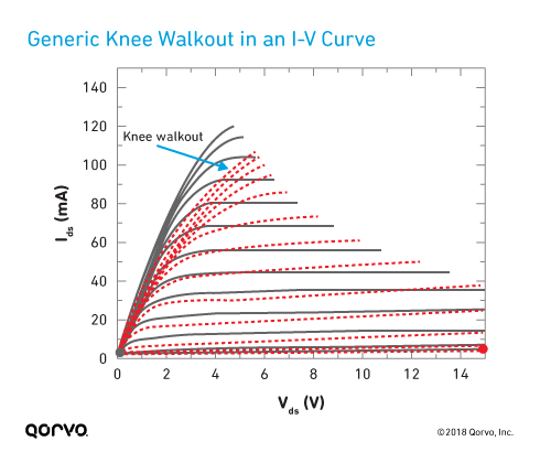
A well-known effect of GaN trapping effect is called inflection point creep, which will shift the inflection point voltage of the IV curve to the right, as shown in the figure below.
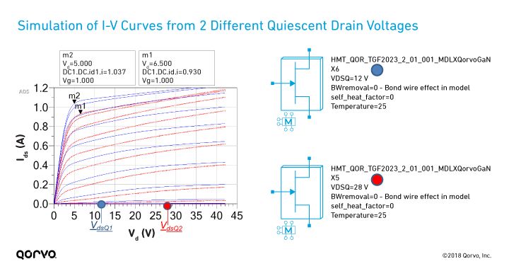
The good news is that nonlinear GaN models can help predict the behavior of this trapping effect. The figure below shows the IV curve of a Qorvo bare die model captured in the Modelithics Qorvo GaN model. It shows the simulation of two different static drain voltages (12 V and 28 V, labeled VdsQ1 and VdsQ2 in the figure below) under short pulse conditions (eg 0.5 µs pulse width at 0.05% duty cycle).
Recreated based on the graphics of the Modelithics Qorvo GaN library
You can see how the inflection point voltage and Imax are affected by the inflection point creep effect associated with the trap. When the self-heating parameter input value is set to zero, the model data well reproduces the IV curve measured under the short pulse conditions of 12 V and 28 V static drain voltage (VgsQ is set to the pinch-off value).
We learned from the above discussion that these two parameters will affect the maximum power of the device accordingly, so the ability of the model to track IV changes with operating voltage will be very important, depending on the application.
Non-linear models can speed up the design process
It is important to understand the impact and nuances of IV curves and their basic limitations and effects on PA design. If you are a novice in this field, I hope this article will help you understand a lot of useful information in the IV curve!
Choosing load conditions to maximize the performance of large signal power is completely different from linear conjugate matching, so using a nonlinear GaN model in the design process can help you get the right design the first time. There is no need to worry too much about matching the output impedance of the transistor. What we need to consider is how to maximize the swing of the current and voltage changes on the IV "runfield", which is controlled by the boundary value of the IV curve, from the inflection point voltage and the maximum current Follow the selected load line down to the pinch-off area.
Ningbo Autrends International Trade Co.,Ltd. , https://www.supervapebar.com