Multiplexed LED drivers help increase efficiency and reduce cost; however, designing multiplexed LED circuits is tricky. Poorly designed circuits can create unwanted LED currents and artifacts in real-world applications. This application note details the issues associated with multiplexed LEDs and explains how to overcome these problems with the MAX6972? MAX6975 family of pulse width modulated LED driver message boards.
Note: The symbol "/" (/MUX1 and /MUX0) indicates the active low function of the MUX1 and MUX0 pins.
The MAX6972–MAX6975 are constant-current LED drivers for high-speed color and video display boards. The MAX6972/MAX6973 can drive up to 16 LEDs or 32 multiplexed LEDs, while the MAX6974/MAX6975 can drive up to 24 LEDs or 48 multiplexed LEDs. The benefit of multiplexing is that it doubles the number of LEDs driven by each drive, thus reducing costs.
However, poorly designed LED multiplex circuits can create artifacts. The LED is in an off state (ie, no current flows), and artifacts can occur when stray current flows through the LED; this results in a very weak display or artifact. These artifact currents typically come from discrete capacitors associated with LED common anode long traces, as well as discrete capacitances caused by LEDs that are slightly forward biased by themselves. With careful multiplexing of circuit design, the MAX6972–MAX6975 family of constant current LED drivers prevent this artifact from appearing in display systems.
Typical multiplexing circuit
Figure 1 shows a typical multiplexing circuit for the MAX6972–MAX6975 (also known as the MAX6972 and MAX6974).
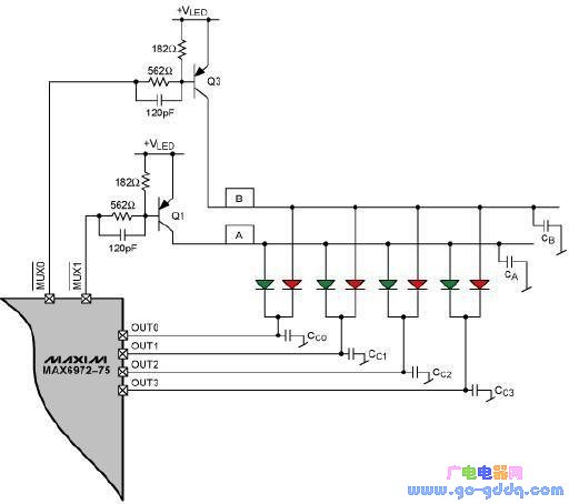
Figure 1. Typical multiplexed circuit, /MUX0 drives the red LED, /MUX1 drives the green LED multiplexed transistors (Q1 and Q3) alternately connected by the MAX6972–MAX6975, while the constant current sink drive pins (OUT0–OUTn) alternately control two The setting between states. In state 1, /MUX1 is low, Q1 is on, and node A is pulled up to VLED, thus all green LED anodes are connected to the LED supply. Similarly, in state 0, /MUX0 is low and Q3 is on, connecting all red LEDs to the VLED supply. The /MUX0 and /MUX1 outputs pass through the open-drain drive circuit, sinking the base current flowing through the 562Ω resistor, turning on the PNP transistor. When /MUX0 and /MUX1 are turned off, the open-drain output is actually an open circuit, allowing the base emitter resistance (each 182 Ω) to turn off the pnp transistor. Between each /MUX0 and /MUX1 state, both Q1 and Q3 turn off 16 internal clock cycles (CLKI), as shown by tEMUX in Figure 2.
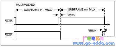
Figure 2. Multiplexed Timing in the Typical Circuit of the MAX6972–MAX6975. In the multiplexed state from /MUX0 to /MUX1, stray current can cause artifacts and vice versa. This effect is most pronounced when the LEDs of the multiplexed circuit are of different colors (lighting wavelengths), so the voltage drop can vary greatly under certain current conditions.
For the sake of simplicity, the multiplexing circuit of Figure 1 is simplified in the discussion that follows, showing only one red and one green LED. In the example below, /MUX0 drives the red LED through Q3, and /MUX1 drives the green LED through Q1.
The voltage drop of the LED is: VRED=2.0VVGREEN=3.1V The power supply is: V+=3.3VVLED=5.0V State 0 can well describe the stray current caused by different forward voltage drop multiplexed LEDs, where /MUX0 is set The bit is low and the red LED is lit (Figure 3).
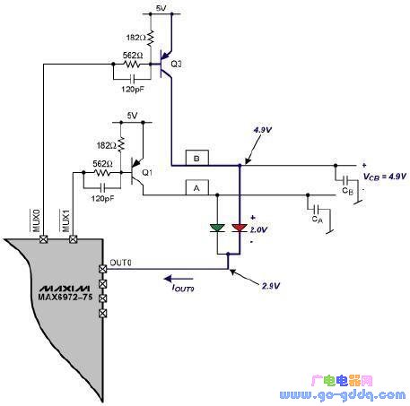
Figure 3. /MUX0 is asserted low, red LED is lit in state 0. After Q3 is turned on, the red LED (node ​​B) anode is pulled up to 4.9V. The current flows through the red LED and the constant current driver (OUT0) of the working port (ie, the channel that drives the LED for any PWM period). The stray capacitance of node B (shown as lumped parameter CB) is charged to 4.9V. The LED cathode is forced to the following voltage, approximately equal to: 4.9V-VRED=2.9V (Equation 1) At the end of state 0, the OUT0 driver stops operating, /MUX0 goes high (inactive), and the anode is disconnected from the LED power supply. Voltage. Since there is no discharge path, the voltage on the red LED PN junction remains close to the 2.0V forward voltage drop. Similarly, since there is no discharge path, the voltage VCB across the stray node capacitance remains at 4.9V. This voltage state remains unchanged during the intermediate state phase of the 16CLKI cycles.
When state 1 begins, /MUX0 is asserted low, Q1 is turned on, the anode of the green LED is connected to 5V, and the OUT0 current driver of the selected LED begins to operate. The final steady state is shown in Figure 4.
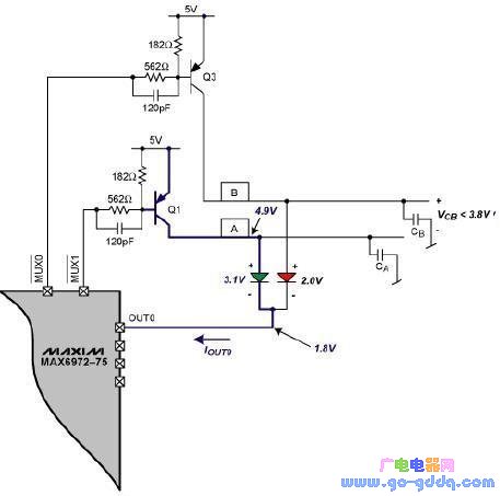
Figure 4. In state 1, the green LED is lit by Q1 and OUT0. The cathode voltage is lower than the green LED voltage drop, which is approximately equal to: 4.9V-VGREEN=1.8V (Formula 2). The 1.8V voltage on the red LED cathode indicates that the anode cannot be high. At 1.8V+VRED=3.8V. At the beginning of state 1, the common cathode voltage (OUT0 voltage in the figure) must be changed from 2.9V to 1.8V. This voltage change requires CB to discharge from 4.9V to 3.8V, or even lower. The CB discharge current flowing through the red LED causes a weak flicker to appear, as shown in FIG.
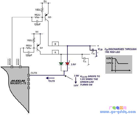
Figure 5. During the multiplexing transition from state 0 to state 1, the stray node capacitance CB to the red LED discharge path causes a weak flicker of the display.
In the previous state, there is always a CB discharge current regardless of whether the red LED is turned "on" or "off". In state 0, the voltage at node B is always charged to 4.9V. Since VRED is less than VGREEN when sharing a common cathode connection, Node B will discharge through the red LED. Depending on the slight difference in forward voltage drop across the various LEDs, CB discharge can cause faint flickering of one or more red LEDs, as shown in Figure 1.
Eliminating artifact currents provides a discharge path for stray node capacitance and sufficient time for discharge to eliminate artifact current. This can be achieved by adding resistors R1 and R2, as shown in Figure 6. In the idle period of the multiplexed state, an appropriate resistance value is selected to achieve sufficient discharge.
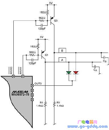
Figure 6. Adding resistors R1 and R2 to the stray node capacitors CB and CA to provide a discharge path.
Resistors R1 and R2 are adjusted to discharge nodes A and B at intermediate state intervals to prevent LED forward biasing when starting the next duty cycle. In the example shown, Node B must be discharged from 4.9V to less than 3.8V before starting state 1.
The intermediate state time is controlled by the system clock frequency, and the maximum clock frequency is 33 MHz. With this maximum frequency, the R2 value can be determined.
The intermediate state time (tEMUX in Figure 2) comes from the system clock frequency: tCLKI = 1/33MHz = 30.3ns (Equation 3) and tEMUX = 16 x tCLKI = 485ns (Equation 4) 150pF per LED (from trace, package The combined capacitance of the lead and the LEDPN junction with a small amount of offset), multiplying the 8 LEDs of each node, can estimate the approximate stray anode capacitance: CB=CA=150pF×8=1.2nF (Equation 5) Substituting into the equation, the discharge current required for CB can be estimated: IDIS_B=CB×ΔVCB/Δt (Formula 6) Substituting the above values ​​into the equation, the discharge current required for CB can be estimated: IDIS_B=1.2 nF×(4.9V-3.8V)/485nsIDIS_B=2.7mA The resistance value of the rated current of 2.7mA is generated at the lowest voltage within the required range: R2=3.8V/2.7mA (Equation 7) R2=1.4kΩ can be applied to IDIS_A Perform the same calculations as CA. However, due to the different effects of the LED forward voltage drop, the artifact current will have different effects when transitioning from state 1 to state 0. In the circuit of Figure 6, it can be seen that the artifact current does not occur when the state 1 to state 0 transitions. However, the values ​​of R1 and R2 are the same, and the red and green LEDs between the /MUX0 and /MUX1 states can be interleaved.
ZGAR AZ Vape Pods 5.0
ZGAR electronic cigarette uses high-tech R&D, food grade disposable pod device and high-quality raw material. All package designs are Original IP. Our designer team is from Hong Kong. We have very high requirements for product quality, flavors taste and packaging design. The E-liquid is imported, materials are food grade, and assembly plant is medical-grade dust-free workshops.
From production to packaging, the whole system of tracking, efficient and orderly process, achieving daily efficient output. WEIKA pays attention to the details of each process control. The first class dust-free production workshop has passed the GMP food and drug production standard certification, ensuring quality and safety. We choose the products with a traceability system, which can not only effectively track and trace all kinds of data, but also ensure good product quality.
We offer best price, high quality Pods, Pods Touch Screen, Empty Pod System, Pod Vape, Disposable Pod device, E-cigar, Vape Pods to all over the world.
Much Better Vaping Experience!


ZGAR AZ Vape 5.0 Pods,ZGAR AZ Vape Pods 5.0,ZGAR AZ Vape Pods 5.0 Pod System Vape,ZGAR AZ Vape Pods 5.0 Disposable Pod Vape Systems
ZGAR INTERNATIONAL(HK)CO., LIMITED , https://www.zgarecigarette.com