The structure of the IC chip supporting the JTAG standard, the principle of boundary scan test, and the method of controlling the IC chip in a specific functional mode by using boundary scan technology are introduced.
The design ideas and methods are given for a certain functional mode of the IC chip, and the PCB board interconnected by two xc9572 pc84 chips is taken as an example for design analysis and experimental implementation. The experiment realizes that the boundary scan technology is easy to debug the circuit system and facilitate the system design, and the designed system control logic is simple and convenient, and easy to implement.
Today, microelectronics technology has entered the era of very large scale integrated circuits (VLSI). With the miniaturization of chip circuits and the development of surface mount technology (SMT) and board assembly technology, traditional test technology faces enormous challenges. In this case, in order to improve the testability of circuits and systems, the Joint Test Action Group (JTAG) proposed a new board test method in 1987, the boundary scan test, which was accepted by the IEEE in 1990. Formed the IEEE 1149.1 standard, also known as the JTAG standard [1]. This technology replaces traditional "physical probes" with new "virtual probes" to improve the testability of circuits and systems. Due to the versatility of the JTAG standard, many IC companies now offer IC chips that support the Boundary Scan mechanism, and even some FPGAs and CPLD chips use this technology.
This paper introduces the structure of the IC chip supporting the JTAG standard, and takes two xc9572_ pc84 chips from Xilinx as an example to explore and use the boundary scan technology to control the IC chip in a certain functional mode, and to target a certain function of the IC chip. The mode design of the chip's JTAG controller.
1 IC chip structure supporting JTAG standardThe core of the boundary scan technology is to set the boundary scan structure between the input and output pins of the IC chip and the core circuit. The JTAG standard defines a 4-wire serial bus [2]. By accessing the boundary scan unit through these four test lines, the purpose of testing the chip core and peripheral circuits can be achieved. Figure 1 shows an IC chip structure supporting the JTAG standard. In the figure, the scan structure consists of a test access channel (TAP), a boundary scan register (BSR), a TAP controller, an instruction register (IR), and an auxiliary register.
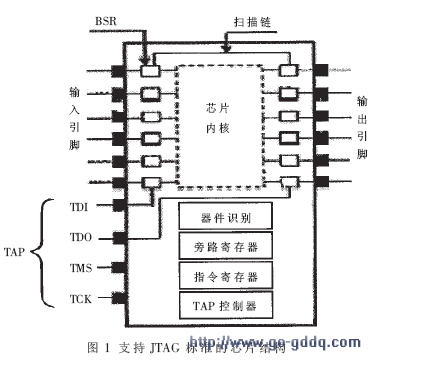
1.1 TAP
The TAP is a test access channel consisting of a 4-wire serial test line. All operations defined by the JTAG standard are controlled by these four test lines. The four test lines are: test clock input line (TCK), test mode select input line (TMS), test data input line (TDI), test data output line (TDO).
1.2 TAP controller
The TAP controller is the core controller for boundary scan testing and has a 16-state finite state machine. It works in sync with the TCK signal and responds to the TMS signal. Under the control of the TCK signal and the TMS signal, the TAP controller can choose whether to use the instruction register scan or the data register scan, and select the various states used to control the boundary scan test. Figure 2 depicts the state transition process of the TAP controller [3].
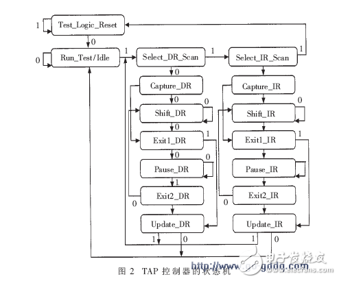
Regardless of the current state, as long as the TMS keeps the five TCK clocks high, the TAP controller will return to the Test_Logic_Reset state, so that the test circuit does not affect the normal logic of the IC chip itself. When a test is required, the TAP controller jumps out of this state, selects the data register scan (Select_DR_SCAN) or selects the instruction register scan (Select_IR_Scan) to enter the various states of Figure 2. A standard test procedure is as follows: The TAP controller captures the instruction information in the Capture_IR state, shifts the new instruction through the Shift_IR state, and the new instruction becomes the current instruction after the Update_IR state. Next, the current instruction selects the corresponding test data register in the Select_DR_Scan state, in Capture_DR. The state captures the response vector of the previous test vector, shifts the response vector out of the Shift_DR state, and moves to the next test vector, loading the new test quantity into the corresponding serial data channel in parallel in the Update_DR state until the last test vector is moved. . Among them, the Pause_DR state and the Pause_IR state suspend the data shift state; and the four Exit states are unstable states, which provide flexibility for state transition.
1.3 BSR
BSR is the core of boundary scan technology, which constitutes a boundary scan chain. Each boundary scan unit (BSC) is composed of a flip-flop Q and a multiplexer mux. Figure 3 shows the structure of the BSC of the BC_1 type in the JTAP standard [3].
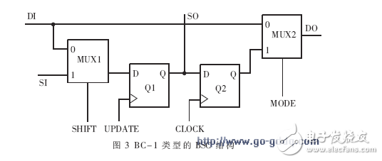
In Figure 3, SI is the serial input of the BSC, connected to the serial output SO of the previous device (BSC), which in turn form a boundary scan chain. The first end of the scan chain is connected to the TDI pin and the end is connected to the TDO pin. When MODE is 0, the chip operates in normal mode. When the chip works in the test mode, the test data enters the multiplexer 1 (MUX1) through the SI terminal under the control of the shift signal (SHIFT=1), and enters the SI end of the next BSC through the SO terminal; When the chip is working in capture mode (SHIFT=0), the flip-flop Q1 will capture the data of the BSR parallel input (DI), send it to the SO end, transfer the captured data in the scan chain, and recover the data in the TDO. Detect the presence of a fault and locate the location of the fault. When MODE is 1, the chip works in the update mode, and the data in Q1 enters the multiplexer 2 (MUX2) under the action of the update signal (UPDATE), and enters the chip through the parallel output (DO) of the BSR. In the kernel.
The RIMA 12V AGM Battery is part of our UN series sealed lead acid battery,
UN series is a high quality lead acid battery, made of 99.997% pure lead, the battery is perfect designed for standby use, but also good at cycle use. The battery is based on AGM battery technology, which means that the electrolyte is absorbed by a fiberglass separator, preventing its leakage, this way the battery can work in any positions.
General Future:
5-12 years design life(25℃)
Non-spillable construction
Sealed and maintenance-free
High reliability and stability
High purity raw material: long life and low self-discharge
Standards:
Compliance with IEC, BS, JIS and EU standards.
UL, CE Certified
ISO45001,ISO 9001 and ISO 14001 certified production facilities
Application:
Uninterruptible Power Supply (UPS)
Emergency backup power supply
Auto control system
Communication power supply
Alarm and security system
Electric Power System (EPS)
12V Battery Rechargeable,12V Battery Small,12V Battery 12Ah,Sealed Lead Acid 12V Battery
OREMA POWER CO., LTD. , https://www.oremabattery.com