Transimpedance amplifiers (TIAs) are front-end amplifiers for optical sensors, such as photodiodes, that convert the sensor's output current to voltage. The concept of a transimpedance amplifier is simple. The feedback resistor (RF) across the op amp uses Ohm's law VOUT = I & TI; RF converts current (I) to voltage (VOUT). In this series of blog posts, I will explain how to compensate TIA and how to optimize its noise performance. For a quantitative analysis of key parameters such as TIA bandwidth, stability, and noise, see the application note titled “Trans Impedance Considerations for High Speed ​​Amplifiersâ€.
In an actual circuit, the parasitic capacitance interacts with the feedback resistor, forming unnecessary poles and zeros in the amplifier's loop gain response. The most common sources of parasitic input and feedback capacitances include photodiode capacitance (CD), op amp common mode (CCM) and differential input capacitance (CDIFF), and board capacitance (CPCB). The feedback resistor, RF, is not ideal and has a parasitic shunt capacitance that can be as high as 0.2 pF. In high-speed TIA applications, these parasitic capacitances interact with each other and also interact with RF to produce an undesirable response. In this blog post, I will explain how to compensate for TIA.
Figure 1 shows a complete TIA circuit with parasitic input and feedback capacitor sources.
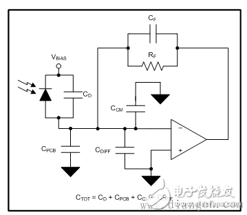
Figure 1: TIA Circuit with Parasitic Capacitance
Three key factors determine the bandwidth of TIA:
Total input capacitance (CTOT).
The ideal transimpedance gain is set by RF.
Op Amp's Gain Bandwidth Product (GBP): The higher the gain bandwidth, the higher the resulting closed loop transimpedance bandwidth.
These three factors are related to each other: For a specific operational amplifier, the positioning gain will set the maximum bandwidth; otherwise, the positioning bandwidth will set the maximum gain.
Parasitic unipolar amplifier
The first step in this analysis assumes that there is a monopolar operational amplifier in the AOL response and the specifications shown in Table 1.
Open-loop gain of op amp at DC and AOL (DC)
120dB
Operational amplifier GBP
1GHz
Feedback resistance RF
159.15kW
Table 1: TIA Specifications
The closed loop stability of the amplifier is related to its phase margin ΦM, which is determined by the loop gain response defined as AOL × β, where β is the reciprocal of the noise gain. The TINA-TITM circuits used to determine the op amp AOL and noise gain are shown in Figure 2 and Figure 3, respectively. Figure 2 configures an open-loop configuration of the test equipment (DUT) to derive its AOL. Figure 3 uses an ideal operational amplifier with ideal RF, CF, and CTOT to derive the noise gain -1/β. FIG. 3 does not currently include parasitic elements CF and CTOT.
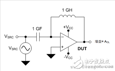
Figure 2: DUT configuration used to determine AOL
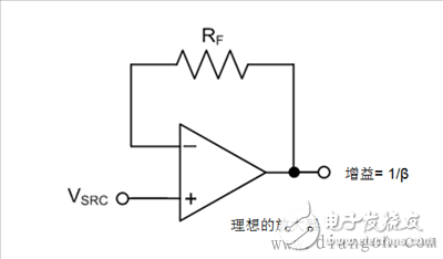
Figure 3: Ideal amplifier configuration to determine noise gain (1/β)
Figure 4 shows the analog amplitude and phase of loop gains AOL and 1/β. Since 1/β is pure impedance, its response is relatively flat in frequency. Since the amplifier is a unity gain configuration as shown in Figure 3, the loop gain is AOL (dB) + β (dB) = AOL (dB). Therefore, the AOL and loop gain curves overlap each other as shown in FIG. Since this is a unipolar system, the total phase shift under fd conditions is 90° due to the presence of AOL poles. The final ΦM is 180°-90°=90° and the TIA is absolutely stable.
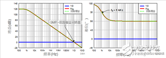
Figure 4: Analog loop gain, ideally AOL and 1/β
Effect of Input Capacitance (CTOT)
Let us analyze the effect of the input capacitance of the amplifier on the loop gain response. Assume that the total effective input capacitance CTOT is 10pF. The CTOT and RF combination will create a zero on the 1/β curve at a frequency of fz = 1/(2πRFCTOT) = 100 kHz. Figure 5 and Figure 6 show the circuit and the resulting frequency response. The AOL and 1/β curves intersect at 10 MHz - the geometric mean of fz (100 kHz) and GBP (1 GHz). The zero point in the 1/β curve becomes the pole in the β curve. The resulting loop gain will have a two-pole response as shown in FIG.
The zero point causes the 1/β amplitude to increase at a rate of 20 dB/decade and intersects the AOL curve at a 40 dB/decade close (ROC) condition, creating potential instability. At 1kHz, the dominant AOL pole exhibits a 90° phase shift in loop gain. At a frequency of 100 kHz, a phase shift of 90° occurs again at zero frequency fz. The final impact is 1MHz. Since the loop gain crossover occurs only at 10 MHz, the total phase shift of fd and fz will be 180°, resulting in ΦM = 0° and indicating that the TIA circuit is unstable.
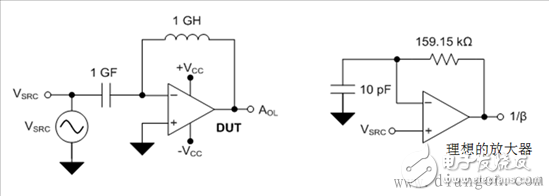
Figure 5: Analog Circuit with 10pF Input Capacitor
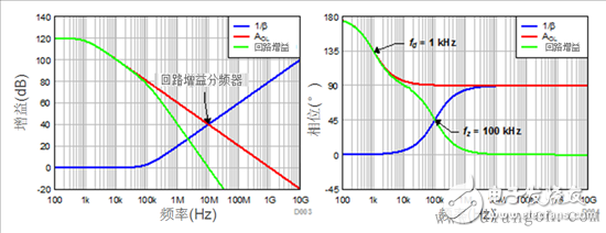
Figure 6: Analog loop gain with input capacitance effects AOL sum (1/β)
Effect of feedback capacitance (CF)
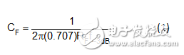
To restore the dephasing due to fz, the pole fp1 is inserted into the 1/β response by increasing the capacitance CF in parallel with RF. Fp1 is at 1/(2πRFCF). To obtain the closed-loop Butterworth response with maximum flatness (ΦM = 64°), use Equation 1 to calculate CF:
Where f-3dB is the closed-loop bandwidth shown in Equation 2:
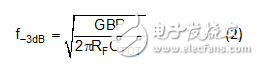
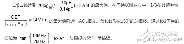
Calculate CF = 0.14pF, f-3dB = 10MHz. Fz is in the 7MHz position. The feedback capacitor includes parasitic capacitance from the printed circuit board and RF. To minimize the PCB, remove the feedback between the amplifier's inverting input and output pins to track the ground and power planes underneath. Use small resistors such as 0201 and 0402 to reduce the parasitic capacitance generated by the feedback element. Figure 7 and Figure 8 show the circuit and the resulting frequency response.
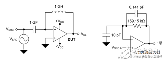
Figure 7: Analog Circuit with a 14 pF Feedback Capacitor
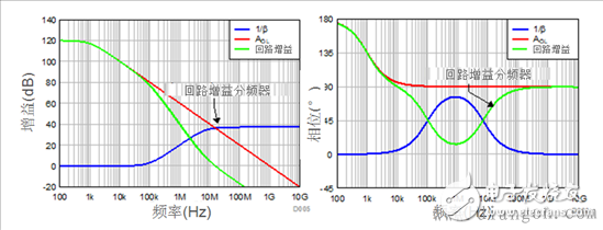
Figure 8: Analog Loop Gain AOL and 1/β with Input and Feedback Capacitor Effects
Table 2 summarizes the inflection points in the loop gain response using the Boolean curve theory.
the reason
Magnitude effect
Phase effect
AOL main pole, fd = 1kHz
Starting at 1kHz, the amplitude drops at a rate of -20dB/dec
At a frequency of 100Hz-10kHz, the phase decreases from 180° at a rate of -45°/dec
Fz = 1/β zero at 100 kHz
Under the influence of fd, the amplitude drops at a rate of -40 dB/dec from 100 kHz
At a frequency of 10kHz-1MHz, the phase drops from 90° to -45°/dec
Fp1 = 1/β pole at 7MHz
With the first two effects, the slope of the loop gain amplitude is reduced from -40ddB/dec to -20dB/dec
Starting at 700 kHz, the phase increases at a rate of 45°/dec and begins to recover. Its impact will continue to increase to 700MHz.
Table 2: Effect of pole and zero on loop gain amplitude and phase
When designing a TIA, customers must understand the capacitance of the photodiode because the capacitance is usually determined by the application. Taking into account the photodiode capacitance, the next step is to choose the right amplifier for the application.
Choosing the right amplifier requires an understanding of the amplifier's GBP, the desired trans-impedance gain and the closed-loop bandwidth, and the relationship between the input capacitor and the feedback capacitor.
Marine Generator with marine diesel engine, marine alternator, control system
. World famous brand marine diesel engine: Cummins, Yuchai, Weichai
. World famous brand alternator: Stamford, Leroy Somer, Marathon, Mecc Alte, Faraday
. Marine control system: Deepsea, ComAp, Deif, SmartGen
. Water Heat Exchanger Type cooling system
Marine Engine,Marine Genset,Marine Generator,Marine Engine Generator
Guangdong Superwatt Power Equipment Co., Ltd , https://www.swtgenset.com