For more than 40 years, PLC has become the backbone of industrial control. Its functions are constantly improving, and its application fields are expanding. It plays an invaluable role in the progress of industrial control technology and social development. With its high reliability and easy operation, PLC has dominated the industrial control industry for decades. Although PLC has its inherent advantages, in the face of constant changes in customer needs, PLC must break through the traditional model in order to survive, and actively seek new changes to adapt to new market development. The embedded PLC with low cost advantage can meet this demand. The so-called embedded PLC refers to PLC that uses SoC embedded system-on-chip and embedded real-time operating system to realize PLC function and can be programmed with IEC61131-3 standard programming language. With the development of high-performance ARM embedded microprocessor, The author designed a new generation of miniature embedded PLC. This paper introduces the architecture of embedded PLC, including its hardware design and software design.
1 Embedded PLC hardware structure design
1.1 Selection of Microcontroller Chips
The CPU is the core of the PLC. It can recognize various commands input by the user according to a specific format, and according to the instruction, according to the current state of the field I/O signal, the corresponding control command is issued to complete the predetermined control task. This design uses the LPC2294 microcontroller from Philips. The LPC2294 is a 32-bit ARM7TDMI-S with real-time emulation and tracking CPU chip with 256kB embedded high-speed flash memory. The 16kB on-chip SRAM.LPC2294 is packaged in a 144-pin package with very low power consumption and many more. Up to 112 general purpose I/O ports, 9 edge or level triggered external interrupt pins, up to 60MHz working crystal, multiple 32-bit timers, PWM unit, real-time clock and watchdog, low conversion time 2.44μs 8-channel 10-bit ADC, 4 advanced CAN interfaces, 2 UARTs (16C550), high-speed I2 C (400kbit/s) and 2 SPI buses. The LPC2294's extensive hardware resources and sophisticated features make this microcontroller ideal for automotive, industrial control applications, medical systems and fault-tolerant maintenance buses.
1.2 The overall structure of the hardware system
This system uses ARM chip LPC2294 as the CPU, designed as the basic mode of 14 PNP type input and 10 way relay output. The overall hardware structure includes:
Power supply and reset module, ARM microcontroller, Flash memory expansion module, digital input and output module, analog input and output module, RS485 interface and CAN interface communication module. The structure of the system is shown in Figure 1.
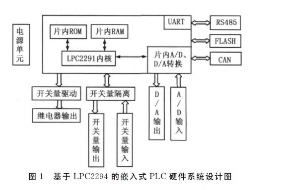
1.2.1 Switching input and output interface circuit
Figure 2 shows a switch input diagram. The front end of this part of the circuit is a first-order filter circuit composed of R and C to prevent external interference signals from entering the system. The input control switch signal (DC 24V) external to the input terminal is input to the input terminal of the photocoupler (PC816) through the input point 10.0 through the current limiting resistor, and M is the common input terminal of the input point 10.0~10.7. Since the P0.23 port is set to the input mode and there is no pull-up resistor inside the port line, an external pull-up resistor is required to prevent the port line from floating. When the 10.0 input is 24V, the photodiode in the photocoupler is turned on, the phototransistor output is pulled low, indicating that the LED of the input state is lit, and P0.23 is set low. When the CPU accesses the signal, the value of the input process image register corresponding to the input point is set to 1.10.0. When the input terminal is 0V, P0.23 is high level, when the CPU accesses the road signal, the CPU The value of the input process image register corresponding to the input point is set to 0. The circuits and working principles corresponding to the other input points are the same.
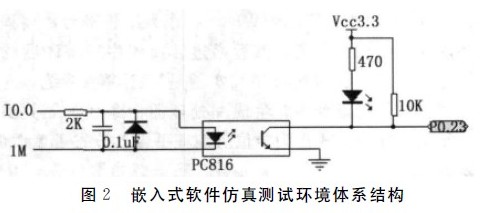
Figure 3 shows the relay output module diagram. The diodes connected in parallel at the ends of the relay coil are used for freewheeling. The working principle of the module is as follows: When the internal output process image register is 1, the LPC2294 port P1.16 outputs 0, the phototransistor is turned on, the relay coil is energized, and the output point is turned on; otherwise, when the internal output process image register is 0. The port P1.16 outputs 1, the relay coil is de-energized, and the output point is disconnected.
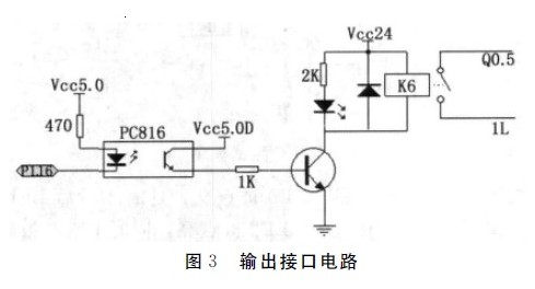
It should be noted that when the GPIO port of the LPC2294 is initially powered on, the voltage of its output port (such as P1.16 in this figure) is unstable, which may cause the external relay to malfunction and cause the external device to work unstable. To this end, we designed the circuit of Figure 4 to improve the stability of the relay output.
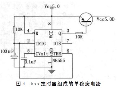
This is a monostable circuit consisting of NE555 timers, where VCC5.0D is terminated with the collector of the optocoupler in Figure 3. The working principle is as follows: the system powers on, the 2, 6 pin levels can not be abrupt, and remain low. Analysis of the internal circuit of NE555 shows that at this time, the output terminal 3 pin outputs a high level, and the circuit starts to charge the R and C circuits. As time goes by, the levels of pins 2 and 6 rise continuously, when it rises to At 23VCC, the output 3 pin will be flipped to a low level to turn the transistor on, and the VCC5.0D output is 5V. Thus, after a period of power-up after the system is powered up, the I/O port level is stabilized, the optocoupler I got electricity and started working. The duration tW of the transient state depends on the magnitude of the external resistor R and capacitor C. tW is equal to the time required for the capacitor voltage to rise from 0 to 23VCC during charging, ie

1.2.2 Analog input circuit design
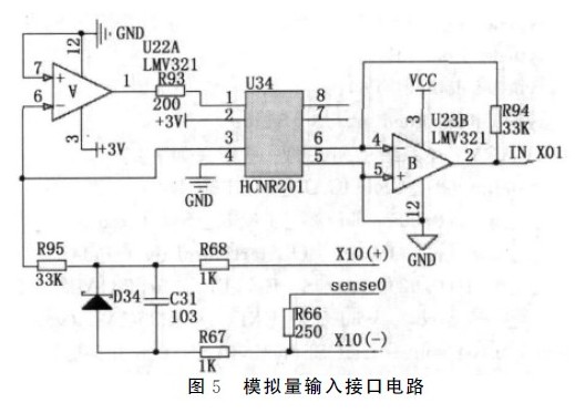
First, through the resistor R66, the current signal output by the field sensor is converted into a 0~5V voltage signal for acquisition. Considering the anti-jamming and protection of the microprocessor circuit, a linear optocoupler HCNR201 is added to the output of the conversion circuit. The hardware circuit is shown in Figure 5.
1.2.3 Serial Communication Interface Circuit Design
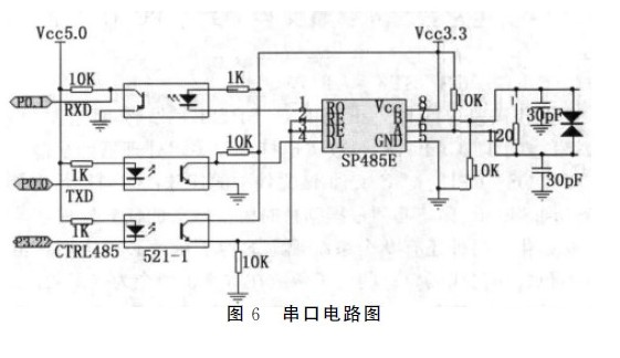
In order to be compatible with other industrial control products, we designed the RS-485 interface standard. In order to convert the TTL level to the RS485 level, the SP485E transceiver was chosen. The SP485E chip's data transfer rate can be as high as 10Mbps, and its biggest feature is the ESD protection circuit provided for the transmitter output and receiver input pins. The interface circuit is shown in Figure 6.
To use these connectors, the ribbon cable is inserted into the Ribbon Connector and the connector is then plugged into the Ribbon Connector on the circuit board. The connectors are designed to provide a secure and reliable connection that can withstand repeated insertions and removals.
Overall, the 2.54mm Ribbon Connectors are an essential component in many electronic devices that require a reliable and secure connection between the ribbon cable and the circuit board.
2.54Mm Ribbon Connector,Pressure Welding Bar Connector,Pressure Welding Bar Connectors,Welding Bar Connector
YUEQING WEIMAI ELECTRONICS CO.,LTD , https://www.weimaicarconn.com