Passive RFID chip H4006 and its application design
1 Introduction of H4006 chip
The working frequency range of H4006 is 10 ~ 15MHz, usually 13.56MHz is used for identification. There is a 64-bit programmable memory in the chip, which can be used to store related information. The information transmission method of H4006 adopts load modulation, the code is Miller code (Miller), and the data transmission rate is 26484 baud (other rates can also be used, but need to be selected in advance). Because H4006 contains resonance circuit and power supply filter capacitor, it is more convenient to use. H4006 is a read-only memory card in wireless mode, and its programming adopts online programming.
2 working principle
2.1 Internal circuit block diagram
H4006 is composed of resonant circuit, clock extraction, frequency division chain, rectifier circuit, power management, memory, Miller code generation, load modulation circuit, etc. Its circuit block diagram is shown in Figure 1.
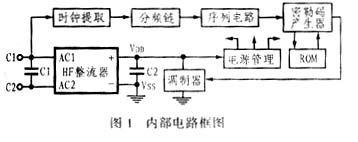
When the rectifier circuit rectifies the coupled RF (13.56MHz) signal and smoothes it through the filter capacitor C2, the power management circuit will activate the internal circuit of the card when the power supply voltage reaches the internal circuit operating voltage. The 13.56MHz signal is divided by the frequency divider chain circuit (The frequency division coefficient is 512), which can generate a clock of 26.484kHz, which is the baud rate of data transmission. If you want to set the frequency division coefficient to 128, 256, 1024, 2048, 4096 or 8192, you need to select it in advance. After the information (64 bits) stored in LASERROM is read out, the Miller code can be generated by the Miller code generator, and at the same time, the Miller code can be used for load modulation and the stored information is sent out.
2.2 Parameter setting of inductance
Inductor L1 is the only external component on the card. Since the resonant capacitor C1 has been integrated into the chip, the inductance value of L1 should be 1.4μH at 13.56MHz. In order to ensure the effect of carrier transmission and load modulation, the Q value should be chosen between 30-40.
2.3 output sequence
The output of card information is usually repeated cyclically in the sequence listed in Table 1. The output sequence is an 82-bit standard information structure (STDMS) plus 9-bit gaps (Pause). The STDMS structure bits use Miller codes, while the 9-bit gap does not use Miller codes. In the gap position, the load modulator switch is in the OFF state, and the gap level is low.
In Table 1, the composition of 64-bit data is as follows:
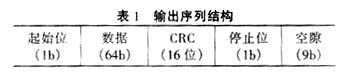
1 to 5 digits are the combination of the chip number. Each chip has a number. They can be set between 1 and 25.
The 6-9 digits are reserved by the manufacturer.
10 to 19 bits are the IC name bits, a total of 10 bits.
20 to 32 bits are user identification (ID) bits, a total of 13 bits, which can be defined by the manufacturer.
33 to 50 digits are extended digits, a total of 18 digits, which is the only system number.
The 51 to 64 bits are the IC position number setting bits, a total of 14 bits, which can be used to indicate the precise position of the processed wafer.
The polynomial generated by the CRC code in Table 1 is x16 + x12 + x5 + 1, which conforms to the CCITT / ISO3309-1984 standard. The CRC code is generated by 64-bit data calculation and can be implemented with a shift register. This register resets to zero at every stop bit.
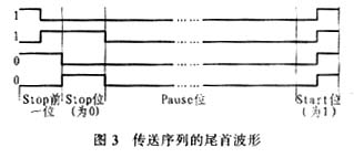
In addition, the start bit in the output sequence is usually logic 1, and the stop bit is logic 0.
2.4 Miller code
In data transmission, the advantage of using Miller code modulation is that Miller code has clock information and has better anti-interference ability.
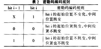
The encoding method of Miller code is shown in Table 2. Its waveform timing is shown in Figure 2.
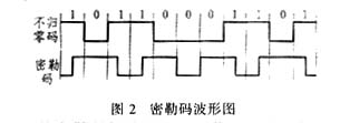
Although the coding rule of the Miller code is that the stop bit is logic 0, its level varies with the coding level of its previous STMDS bit. The 9-bit Pause bit can be used to lower the level so that the start bit has the same form. Figure 3 describes this clearly.
3 Application Design
Figure 4 shows the block diagram of the H4006 application system. The system consists of a card and a card reader. Since H4006 is a storage card, data transmission is only transmitted from the card to the card reader, so there is no coding and modulation circuit in the card reader, only the demodulation and decoding circuit is required.
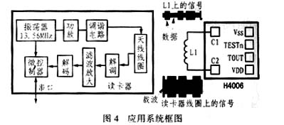
H4006 has 6 pins. When the radio frequency works, it is read-only, and the inductor L1 can be connected to the C1 and C2 pins. During data transmission, the waveforms on the card and card reader antenna coil are shown in the figure. This waveform is generated by the load modulation in the card. . The other four pins of H4006 are used for testing. VDD and VSS are the positive and negative terminals of the power supply, and TESTn and Tout are the test input and output terminals.
Figure 5 shows the 13.56MHz oscillator and power amplifier circuit in the card reader. In the figure, the power amplifier circuit uses a high-efficiency Class E (Class E) amplifier, so the impedance of the L1 choke should be large enough, and the ICC flowing through it should be constant, and C5 is used to improve the performance of the amplifier. Eliminate the effect of the transistor's own output capacitance. When the transistor is in the switching state, the efficiency of the entire amplifier is extremely high. The resonant frequency of the series resonant circuit formed by L3 and C9, C11, and C10 in the figure is 13.56MHz. This loop should have a high Q value to ensure that the output carrier is a sine wave. In fact, L3 is also the coupling coil of the card reader, and the carrier electromagnetic field it generates should meet the requirements of the non-contact IC card technical standards. L2 and C8 are used to block higher harmonics.

13. The 13.56MHz oscillation signal generated by the 56MHz crystal oscillator is used as the clock of the CPU in the card reader, and the other way can be used to drive the Class E amplifier after amplification.
Send the load modulation signal on L3 from C7 to the demodulation and decoding circuit to get the data. The demodulation can use the envelope detection method to restore the Miller code obtained after demodulation to the non-return-to-zero code with the Miller code decoder and send it to the microcontroller, and send it to the PC from the serial port.
Weatherproof/Waterproof Type F Outlets
"Waterproof Type F Outlets Black,Waterproof Type F Outlets,Waterproof Outlet Plug,Waterproof Exterior Outlet "
Yang Guang Auli Electronic Appliances Co., Ltd. , https://www.ygpowerstrips.com