Switch power supply various protection circuit examples detailed anatomy!
Input undervoltage protection circuit
1 Overview (Circuit Type, Main Function Description):
This circuit belongs to the input undervoltage circuit. When the input voltage is lower than the protection voltage, it will pull down the power supply Vcc of the control chip, thereby turning off the output.
2 circuit composition (schematic diagram):
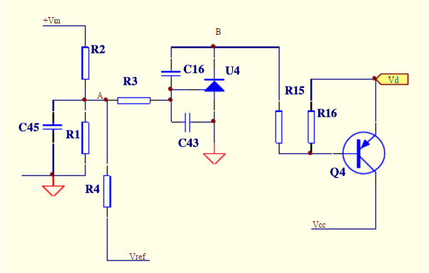
Input undervoltage protection circuit II
1 Overview (Circuit Type, Main Function Description):
Input undervoltage protection circuit. When the input voltage is lower than the set undervoltage value, the output is turned off; when the input voltage rises to the set recovery value, the output automatically returns to normal.
2 circuit composition (schematic diagram):

3 working principle analysis (main function, performance index and realization principle):
When the input voltage is within the normal operating range, Va is greater than the voltage regulation value of VD4, VT4 is turned on, Vb is 0 potential, VT5 is cut off, at this time, the protection circuit does not work; when the input voltage is lower than the set undervoltage value, Va Less than VD4 regulator, VT4 is off, Vb is high, VT5 is on, COMP (pin 1 of the chip) is pulled to 0 potential, the chip shuts down the output, thus achieving undervoltage protection. R21, VT6, and R23 constitute a hysteresis circuit for undervoltage shutdown and recovery. When the undervoltage turns off, VT6 turns on and parallels R21 and R2.
When recovery, VT6 cuts off, 
4 advantages and disadvantages of the circuit
Advantages: Simple circuit form and low cost.
Disadvantages: Due to the difference in the voltage regulation value between the VD4 batch of the voltage regulator, the undervoltage protection point is floating up and down, and the relevant parameters must be frequently debugged during mass production.
5 Application Notes:
VD4 should select a regulator with a better temperature coefficient. Components that need to be debugged, such as R2, should be considered in parallel to facilitate debugging.
Output overvoltage protection circuit
1 Overview (Circuit Type, Main Function Description):
Output overvoltage protection circuit. When an applied voltage higher than the normal output voltage range is applied to the output or the circuit itself fails (open loop or otherwise) causing the output voltage to rise above the regulation value, the circuit clamps the output voltage at the set value.
2 circuit composition (schematic diagram):
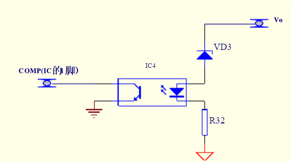
3 working principle analysis (main function, performance index and realization principle):
When the output voltage is over-voltage, when the voltage applied to VD3 is greater than its regulation value, VD3 turns on, the output voltage is clamped, and at the same time, it feeds back to the primary through IC4.
4 advantages and disadvantages of the circuit
Advantages: The circuit is simple in form and low in cost.
Disadvantages: Due to the difference in the voltage regulation value between the VD3 batch of the voltage regulator, the overvoltage clamp point floats up and down, and the relevant parameters must be frequently debugged during mass production.
5 Application Notes:
VD3 should select the regulator with better temperature coefficient. Components that need to be debugged, such as R32, should be considered in parallel to facilitate debugging.
When the overvoltage protection circuit works, the circuit is in abnormal operation. For a circuit with output voltage up-down function, the overvoltage protection point should be greater than the maximum value of the output voltage up-regulation.
Output overvoltage protection circuit II
1 Overview (Circuit Type, Main Function Description):
Output overvoltage protection circuit. When an applied voltage higher than the normal output voltage range is applied to the output terminal or the circuit itself is faulty (open-loop or otherwise) causing the output voltage to rise above a normal value, the circuit stabilizes the output voltage at a set value.
2 circuit composition (schematic diagram):
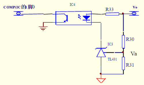
3 working principle analysis (main function, performance index and realization principle):
When the output voltage is overvoltage, Va>Vref, IC3 is turned on, and the output voltage is stabilized at the set overvoltage protection value by IC4 feeding back to the primary side.
4 advantages and disadvantages of the circuit
Advantage: The output overvoltage protection value can be set accurately.
Disadvantages: The relative voltage regulator clamp costs slightly higher.
5 Application Notes:
When the overvoltage protection circuit works, the circuit is in abnormal operation. For a circuit with output voltage up-down function, the overvoltage protection point should be greater than the maximum value of the output voltage up-regulation.
Overvoltage protection self-locking control circuit
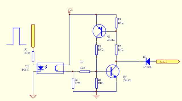
3 working principle analysis (main function, performance index and realization principle):
The above figure shows an isolated self-locking control circuit. When the overvoltage protection signal CONTROL terminal gives a high level, the transistor in U1 turns on and VCC is the power supply end of the entire circuit. Vcc supplies a base current to R2 through R5. Q1 turns on and goes into saturation. SHUT is pulled low by Q2 and PWM turns off the power supply. Q2 controls the conduction of Q1 at the same time. When Q2 is turned on, the base current of Q1 goes to ground through R2, Q1 turns on, and then provides a base current to Q2 via R3 to maintain the conduction of Q2. Q1 and R1, R2, and R3 constitute the positive feedback circuit of Q2.
4 advantages and disadvantages of the circuit
Advantages: Effective self-locking protection, the entire circuit is equivalent to a SCR.
Disadvantages: The entire circuit requires a fixed Vcc. When there is no power supply at the PWM power supply, it is also necessary to ensure the presence of the VCC voltage in the above figure.
5 Application Notes:
1. This circuit must have continuous power supply self-locking to be effective.
2. This circuit should not be used in unattended power systems.
Over-temperature protection circuit
1 Overview (Circuit Type, Main Function Description):
The circuit is an over-temperature protection circuit, but when the temperature is higher than the set protection point, the module output is turned off, and the module is automatically turned on when the temperature is restored.
2 circuit composition (schematic diagram):

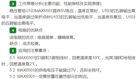
Over-temperature protection circuit - thermistor
1 Overview (Circuit Type, Main Function Description):
This circuit uses a thermistor to detect the temperature of the substrate. The resistance of the thermistor changes with the temperature of the substrate. The change of the resistance of the thermistor causes the input voltage of the op amp to change, thereby achieving the output of the op amp flip control PWM chip, and then The module is closed.
2 circuit composition (schematic diagram):
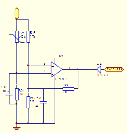
3 working principle analysis (main function, performance index and realization principle, calculation and analysis of key parameters):
R99 thermistor is negative temperature coefficient thermistor, at room temperature, R99 = 100k, R99 and R94 partial pressure 0.45V is U2 op amp negative input, much lower than the op amp's positive input 2.5V (R23 and R97 points Pressure), so the output of the op amp is high, no effect on the SS side of the LM5025, and the module is operating normally.
As the substrate temperature increases, the resistance of R99 decreases. When the value is decreased to a certain value, the negative input of the op amp is greater than the positive input, and the output of the op amp is low, the SS of the LM5025 is pulled low, thus closing the module. Output; temperature protection point can be adjusted appropriately R94, R23, R97 resistance and adjust accordingly.
After the module closes the output (over-temperature protection), the substrate temperature will decrease, the R99 resistance will increase, and the negative input of the op amp will decrease. To make the op amp turn over normally, the resistor R98 is introduced. The principle is that the op amp output is low. R98 is equivalent to connecting in parallel with R97, lowering the reference of the op amp and pulling the voltage gap between the positive and negative input of the op amp, thus realizing the temperature hysteresis. For example, when the substrate temperature is 90°C, open it at 80°C.
4 Key parameters calculation and analysis
4.1 op amp positive input voltage: VR97=Vref2=5/(1+R23/R97)=5/(1+10/10)=2.5V
4.2 op amp negative input voltage VR94+0.007=VR97=5*R94/(R99+R94)+0.007,
4.3 The resistance value of the thermistor when temperature protection is obtained: R99(t)=(Vref*R24/(Vref*R97/(R23+R97)-0.007))-R94
4.4 Calculations when considering tolerances are shown in the table below:
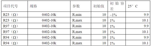
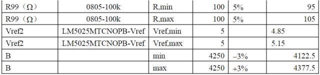
4.5 Value of R99 when over temperature protection
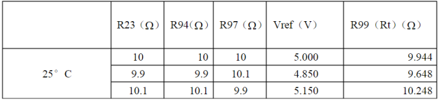
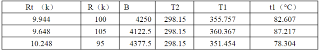
4.6 R99-SDNT2012X104J4250HT(F) is a thermistor with a negative temperature coefficient, 100k at 25°C, and over-temperature protection with a resistance of about 10k (see table above). The calculated temperature is:
Rt=R*e(B(1/T1-1/T2)) T1=1/(ln(Rt/R)/B+1/T2))
T2: room temperature 25°C, T2 = 273.15 + 25 = 298.15 in the above formula; B: 4250 ± 3%; R: resistance value at 25°C, 100k, the calculated T1 value is also added after 273.15, Therefore, in the following table, t1=T1-273.15 is in degrees Celsius. Rt: resistance after temperature change, 10k, 9.704k, 10.304k, see table above
4.7 Return difference
After the op amp output is low, resistor R98 (51k) is on R97 and the reference is pulled low. The new reference voltage Vref1=Vref*(R98//R97)/(R23+R98//R97)=2.28V reaches 2.44 At V, the resistance of R99 is R99=Vref*R94/Vref1-R94=11.9k When R99 reaches 10.49k, the temperature is calculated according to the following table
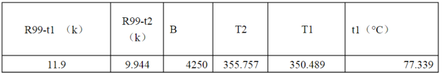
Temperature difference = 82.6-77.3=5.3°C
5 advantages and disadvantages of the circuit
Advantages: Temperature protection point and temperature difference can be adjusted
Disadvantages: Low temperature accuracy
Circuit is slightly more complicated than using temperature switch
Temperature protection reflects the temperature of the substrate near the thermistor and does not reflect the highest device temperature of the module, but this can be resolved at design time. For example, the substrate temperature is protected at 90°C, and the maximum temperature of the device on the actual board has reached 130°C. The temperature protection point can be properly adjusted to provide protection.
6 Application Considerations
Place the thermistor near the heating device as much as possible.
A comprehensive selection of USB connectors are available with various combinations of form factors, interface and version types, vertical and horizontal configurations, as well as a unique new USB 2.0 Type-C charging option. Chances are Antenk have the right USB connector for you.
USB (Universal Serial Bus) was originally developed and introduced in 1996 as a way of setting up communication between a computer and peripheral devices by replacing many varieties of serial and parallel ports.
USB connectors have become the standard connection method for devices such as mice, keyboards, game pads & joysticks, scanners, digital cameras, printers and external hard drives.
Although designed for personal computers USB has become commonplace on other devices such as mobile phones, PDA's, video game consoles, AC power adaptors, memory sticks and mobile internet access dongles.
USB Connector Type
USB Type A
Also known as USB standard A connector, the USB A connector is primarily be used on host controllers in computers and hubs. USB-A socket is designed to provide a "downstream" connection intended for host controllers and hubs, rarely implemented as an "upstream" connector on a peripheral device. This is because USB host will supply a 5V DC power on the VBUS pin. As such, it is important to remember while purchasing USB cables it is safest to make sure at least one of the plugs is a USB A.
Though not that common, USB A male to A male cables are used by some implementers to make connections between two USB A style female port. Be aware that typical A-A cables are not intended for connection between two host computers or computer to hub.
Related Products:
USB 2.0 A to A Female Cables
USB 2.0 A to B Cables
USB 2.0 A to Mini B Cables
USB 2.0 A to Micro B Cables
USB 2.0 A to A Angle Cables
USB 2.0 A to B Angle Cables
USB 2.0 A to Mini B Angle Cables
USB 2.0 A to Micro B Angle Cables
USB 2.0 A to B Locking Cables
USB 2.0 A to Mini B Angle Cables
USB 2.0 A Female to A Cables
USB 2.0 A Female to Crimp Housing Cables
USB 2.0 A to B High Flex Cables
USB 2.0 A to C Cables
USB Type B
Also known as USB standard B connector, the B style connector is designed for USB peripherals, such as printer, upstream port on hub, or other larger peripheral devices. The primary reason for the development of USB B connectors were to allow the connection of peripheral devices without running the risk of connecting two host computers to one another. USB B type connector is still used today, though it is slowly being phased out in favor of more refined usb connector types.
Related Products:
USB 2.0 A to B Cables
USB 2.0 A to B Angle Cables
USB 2.0 A to B Locking Cables
USB 2.0 A to Mini B Angle Cables
USB 2.0 B Female to B
USB 2.0 B Female to 5 Pin Cables
USB Type C
USB-C or USB Type-C connector is the newest USB interface came to the market along with the new USB 3.1 standard. Different from previously mentioned USB A type and B type connector, USB C Type connector can be used on both host controller ports and devices which use upstream sockets. In the last few years a numbers of laptops and cellphones have appeared on the market with C style USB connectors.
USB Type C connector is compatible with USB 2.0, 3.0, 3.1 Gen 1 and Gen 2 signals. A full feature USB 3.1 Gen 2 C to C cable is able to transmit data at maximum 10 Gbps with enhanced power delivery of up to 20V, 5A (100W) and to support DisplayPort and HDMI alternate mode to transfer video and audio signal.
Related Products:
USB-C to USB-C Cables
USB 3.0 to USB-C Cables
USB Mini B
Similar to USB B type connector, USB mini B sockets are used on USB peripheral devices, but in a smaller form factor. The mini B plug by default has 5 pins, including an extra ID pin to support USB On-The-Go (OTG), which allows mobile devices and other peripherals to act as a USB host.
Initially, this plug was designed for earlier models of smartphones, but as smartphones have become more compact and with sleeker profiles, the Mini USB plug has been replaced by the micro USB. Now, the Mini-B is designed for some digital cameras while the rest of the mini plugs series have become more of a legacy connectors as they are no longer certified for new products.
Related Products:
USB 2.0 A to Mini B Cables
USB 2.0 Mini A to Mini B Cables
USB 2.0 Mini B to Mini B Cables
USB 2.0 Mini B to Mini B Female Cables
USB 2.0 Mini A to Mini B Angle Cables
USB 2.0 A to Mini B Locking Cables
USB 2.0 A to Mini B High Flex Cables
USB 2.0 Mini B to Mini B High Flex Cables
USB Micro B
The micro USB B connector essentially a scaled down form of the mini USB which allowed mobile devices to get slimmer while still maintaining the ability to connect to computers and other hubs.
USB A-Type Connector, USB B-Type Connector, USB Type-C Connector, Micro-USB A Connector, Micro USB B Connector, USB Mini-b (5-pin) Connector, USB Mini-b (4-pin) Connector, USB 3.0 A-Type Connector, USB 3.0 B-Type Connector, USB 3.0 Micro B Connector
ShenZhen Antenk Electronics Co,Ltd , https://www.antenkcon.com