With the rapid development of integrated circuit technology, the development of semiconductor memory, microprocessors and other related technologies has been rapidly developed. FPGA is widely used in electronic design for its characteristics of strong reliability, fast operation, and parallelism. As a kind of programmable logic device, FPGA has evolved from the peripheral device of electronic design to the core of digital system in just 20 years. With the advancement of semiconductor process technology, FPGA device design technology has achieved rapid development and breakthroughs.
The divider is usually used to divide a given clock frequency to get the desired clock frequency. In designing a digital circuit, a plurality of clock pulses of different frequencies are often used, and the clock frequency division is generally performed by using a fixed crystal clock frequency to generate clock pulses of different frequency required.
In FPGA design, the frequency divider is a basic design with a relatively high frequency. In many designs, chip-integrated phase-locked loop resources are often used. For example, Xilinx's DLL and Altera's PLL are used to divide the clock. , multiplier and phase shift. In some cases where the accuracy of the clock is not high, the hardware description language is often used to clock the clock source.
A frequency divider is a basic circuit and generally includes a digital frequency divider, an analog frequency divider, and an RF frequency divider. According to the needs of different designs, it is sometimes required to equalize the duty cycle. The digital divider uses the principle of a counter and the weight value is the frequency division factor. The analog divider is a frequency divider that is implemented with a band-stop bandpass (such as a speaker with a high, medium, or low horn on the speaker). The RF divider is also a filter principle and is implemented with internal and external attenuation and impedance matching.
With the development of FPGA technology, hardware design digital frequency divider based on FPGA technology has become the research focus of digital system design. Digital dividers are usually divided into integer dividers and fractional dividers. Fractional dividers are also required under some requirements.
This design is a digital frequency divider based on FPGA. Through the VHDL hardware design language, the designed frequency divider is simulated and verified on Modelsim6.5.
2. Digital divider designThe design of the digital divider is different from that of the analog divider. The digital divider can use a flip-flop design circuit to clock the clock pulses. An important indicator of the frequency divider is the duty cycle, which is the ratio of high-level pulses in the entire cycle in one cycle. Duty cycle generally has requirements of different ratios such as 1:1, 1:N, etc. Since the ratio of duty ratios is not the same, the clock division principle used is also different. In the FPGA digital divider design, it is mainly divided into integer divider, fractional divider and fractional divider. The design of the integer divider, the design of the fractional divider, and the design of the fractional divider are now described separately.
2.1 Integer divider design
An integer divider is an integer multiple of the reference clock and the desired clock frequency. The division type of the integer divider generally includes an odd division and an even division. Although the clock division principle may vary depending on the clock division requirements, the standard counter principle can be used.
The design principle of even-numbered frequency dividers is relatively simple, mainly using counters. Assume that n (n is even) frequency division is performed, and a counter cycle count triggered by the rising edge of the divided clock is implemented. When the counter value is 0-((n/2)-1), the output clock signal is inverted, and the counter is given a reset signal at the same time, so that when the next clock rising edge comes, the counter restarts counting, and thus continuously loops.
The design principle of the odd-numbered frequency divider is very similar to the design method of even-numbered frequency-dividing, and is implemented by a counter. If n (n is an odd number) frequency division is to be performed, an n-ary counter can be directly designed. Another method is to select two counters, cnt1 and cnt2, to trigger counting on the rising and falling edges of the clock. Both cnt1 and cnt2 when the counter value is 0-((n/2)-1), the output clock signal is inverted, and the counter is provided with a clock reset signal, so that when the next clock rising edge comes, the counter restarts counting, so Cycle through. It can be seen that the counters cnt1 and cnt2 are implemented in the same way except that the inverting edges are not the same and the final output clock is clkout = clk1 + clk2.
2.2 Design of Fractional Frequency Divider
The basic principle of fractional frequency division is to use an impulse throughput counter and phase-locked loop technique to first design two integer dividers with different frequency division ratios, and then obtain the required number of times by controlling the number of different frequency division ratios per unit time. When the fractional frequency is divided and the frequency division coefficient is N-0.5 (N is an integer), the time for subtracting the pulse can be controlled so that the output becomes a stable pulse frequency instead of a N frequency division and a N-1 frequency division.
Fractional dividers come in a variety of designs, but the basic principle is the same, all of which take a number of cycles to divide a few cycles into counts or counts, resulting in an entire count cycle. A fractional divider ratio is obtained on the overall average. Another method of frequency division is to use state machines and counters. Assuming that the frequency of the clock signal is 1khz, it is necessary to generate a divided signal of 750khz with a frequency division factor of 6/8. The basic design idea is to reserve 6 clock signals in 8 clock signals. This method requires the number of state machines to be set in advance, and is mainly used when it is known which fractional frequency division coefficient needs to be used. If the frequency division factor changes, it needs to be modified inside the program.
The design method of the dual-modulus pre-decimal frequency division is assuming that the m and n clocks are divided (where m and n are integers and n is 10). Since there is only one decimal point, a total of 10 frequency divisions are performed. . The general rule is: Perform n times of m+1 frequency division and 10n times of m frequency division. For example, design a frequency divider with a frequency division factor of 3.6, and multiply the fractional part of 6 by a factor of 2, assume that the accumulated value is a, if a is 10, then divide by 3, if a 10 times 6. After that, if a ′′=10, then divide by 4 and divide by 4 and then subtract 4 from the cumulated value to compare with 10 to determine whether the next frequency division is 4 or 3, so that the frequency divider is designed to Six times with 4 frequency divisions and 4 times with 3 frequency divisions, the total frequency division value is (6&Times; 4+4&Times; 3)/(6+4) = 3.6.
2.3 Design of fractional divider
The data input portion of the fractional divider is basically the same as the fractional frequency divider, and the only difference is that the digital tube display portion shows the three-way frequency division coefficient. Since the score can be converted into decimals for calculation under certain conditions, the design idea of ​​fractional frequency division is very similar to the fractional frequency division. Assuming that the frequency is divided, the total frequency is determined by the denominator m. The rule is to perform n times j+1 frequency division and mn times frequency division j. The two frequency divisions are alternately performed in a manner similar to fractional frequency division. Whether the cumulative result is greater than or equal to the denominator or less than the denominator determines whether to divide by j or j+1.
3. Digital divider FPGA design and simulationUsing the FPGA to clock the 8192 kHz reference clock, the clock frequencies of 1024 kHz, 512 kHz, 256 kHz, and 1 kHz are obtained, respectively, and they need to be divided by 8, 8, 16, and 8,192 respectively. When using an FPGA to design an integer divider, the VHDL hardware description language is implemented using a counter method.
3.1 1024kHz Clock Divider
According to the required clock frequency of 1024 kHz, and the frequency of the crystal clock is 8192 kHz, the crystal clock and the required clock frequency are exactly 8 times the integral multiple, so the 8192 kHz crystal clock needs to be divided by 8 to obtain the result. Needed clock. According to the principle of integer multiplier design method, through the ISE 9.1 logic design tool, the VHDL hardware description language is used to design the frequency divider of the 8 frequency division. However, 8 is an even number, so an even-numbered divider needs to be designed. The contents of the design were verified by Modelsim6.5 simulation software. The results are shown in Figure 3-1.
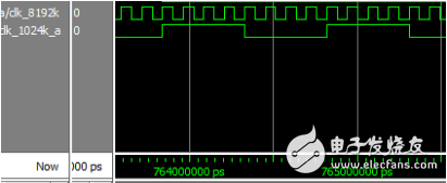
Figure 3-1 1024kHz Clock Divider
According to Fig. 3-1, when 8192 kHz crystal clock is input to 8 clocks, the system outputs 1 clock, which is a 1024 kHz frequency clock. The counter is used in program design. When the counter value is 0-((n/2)-1)=-3, the output clock signal is toggled and the counter is given a reset signal so that the next clock rises. The counter resumes counting and continues to cycle.
3.2 512kHz clock divider
According to the required clock frequency of 512 kHz clock, and the frequency of the crystal clock is 8192 kHz, the crystal clock and the required clock frequency happen to be an integral multiple of 16 times, so the 8192 kHz crystal clock needs to be divided by 16 to obtain the result. Needed clock. According to the principle of integer multiplier design method, through ISE 9.1 logic design tool, VHDL hardware description language is used to design a frequency divider with a frequency divider of 16. However, 16 is an even number, so an even-numbered divider needs to be designed. The contents of the design are verified by Modelsim6.5 simulation software. The result is shown in Figure 3-2.
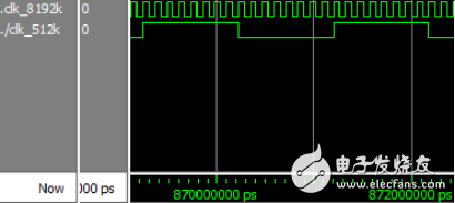
Figure 3-2 512 kHz Clock Divider
According to Figure 3-2, when the 8192kHz crystal clock is input to 16 clocks, the system outputs 1 clock, which is a 512kHz clock. The counter is used in program design. When the counter value is 0-((n/2)-1)=-7, the output clock signal is inverted, and the counter is given a reset signal to make the next clock rising edge come. The counter resumes counting and continues to cycle.
3 .3 256kHz Clock Divider
According to the required clock frequency of 256 kHz clock, and the frequency of the crystal clock is 8192 kHz, the crystal clock and the required clock frequency happen to be an integral multiple of 32 times, so the 8192 kHz crystal clock needs to be divided by 32 to obtain the result. Needed clock. According to the principle of integer multiplier design method, through the ISE 9.1 logic design tool, use VHDL hardware description language to design 32-way divider. However, 32 is an even number, so an even-numbered divider needs to be designed. The contents of the design are verified by Modelsim6.5 simulation software. The result is shown in Figure 3-3.
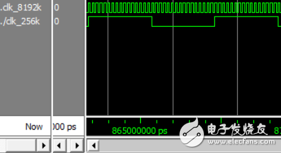
Figure 3-3 256 kHz Clock Divider
According to Fig. 3-3, when the 8192kHz crystal clock is input to 32 clocks, the system outputs 1 clock, which is a 256kHz clock. The counter is used in program design. When the counter value is 0-((n/2)-1)=-15, the output clock signal is toggled and the counter is given a reset signal so that the next clock rises. The counter resumes counting and continues to cycle.
3.4 1kHz clock divider
According to the required clock frequency of 1 kHz clock, and the crystal clock frequency is 8192kHz, the crystal clock and the required clock frequency is exactly 8192 times the integer multiple relationship, so you need to 8192kHz 8192kHz crystal clock frequency to obtain the Needed clock. According to the principle of design method of integral multiple frequency divider, through the ISE 9.1 logic design tool, use VHDL hardware description language to design the frequency divider of 8192 frequency division. However, 8192 is an even number, so an even-numbered divider needs to be designed. The contents of the design are verified by Modelsim6.5 simulation software. The results are shown in Figure 3-4.
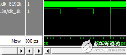
Figure 3-4 1kHz Clock Divider
From Figure 3-4, when the 8192kHz crystal clock is input to 8 clocks, the system outputs 1 clock, which is a 1kHz frequency clock. The counter is used in program design. When the counter value is 0-((n/2)-1)=-4095, the output clock signal is toggled and the counter is given a reset signal so that the next clock rises. The counter resumes counting and continues to cycle.
4 ConclusionThis article presents a digital divider design method based on FPGA. A counter design method was used to divide the 8192 kHz reference clock and obtain clock frequencies of 1024 kHz, 512 kHz, 256 kHz, and 1 kHz, respectively. Other even multiples can also be divided to the desired frequency clock in a similar manner. The correctness of the design was verified by the Modelsim6.5 simulation tool.
Heated Desk Pad,Warm Desk Pad,USB Heated Desk Pad,Warm Office Desk Pad
Ningbo Sinco Industrial & Trading Co., Ltd. , https://www.newsinco.com