Due to the special working environment of the fire control system, the required acquisition signals are complex and diverse, and traditional acquisition systems based on microcontrollers or PCs are often difficult to perform. Aiming at the above problems, a design scheme of data acquisition system based on STM32+FPGA is proposed. This scheme can not only complete real-time and accurate acquisition of multiple signals, but also has high-speed signal processing and data transmission capability. Small size, abundant resources, and low price.
1, the overall design of the systemIn practical applications, the collected signals have both analog signals and digital differential signals, and are characterized by multi-channel, serial and mixed, and large data volume. In order to meet the demand, this paper designs the data acquisition system shown in Figure 1, which can collect, process and real-time transmission of 6 ±10V analog signals and 18 digital differential signals according to requirements. The system adopts the combination of STM32+FPGA. The FPGA is the EP1K50TC144 device of ALTER Company. The STM32417 sends control commands to the FPGA, realizes signal acquisition through the internal address decoding, logic control and data buffer of the FPGA, and notifies STM32417 to read the data. Finally, The obtained data is processed and transmitted by STM32417.
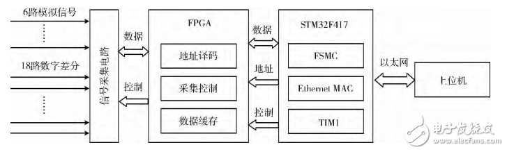
Figure 1 Overall design
Among them, STM32F417 is a microcontroller based on ARM-CoRTEX-M4 architecture produced by STMicroelectronics. It has advanced core architecture, superior performance, frequency up to 168MHz, high execution efficiency, high computing power and data processing capability. Has a wealth of peripheral interfaces and extensions. In Figure 1, the Ethernet communication between the STM32F417 and the host computer is the MII external DP83848 physical layer chip, which is implemented by the relevant configuration and extension.
2, STM32 and FPGA interface designThere are many ways to interface between STM32F417 and FPGA. It can be serial or parallel. Considering the obvious advantage of FPGA in multi-channel parallel data processing [5,6], the design uses STM32F417 variable static storage control. The FLEXIBLESTATICMEMoRyCoNTRoLLER (FSMC) parallel bus interface enables connection to the FPGA.
2.1, interface circuit designFSMC is a new type of memory expansion technology used in the STM32 series. It supports different external memory types, including many types of static memory. Therefore, the FPGA can be configured as an external SRAM of the STM32F417. The address/control three bus is used to achieve the operation, which ensures fast operation speed and high flexibility. The interface circuit hardware connection is shown in Figure 2.
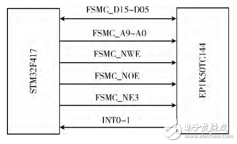
Figure 2 STM32F417 and FPGA interface connection circuit
Electric Junction Box,Waterproof Junction Box,Junction Box Wiring,Pvc Junction Box
CIXI MEMBRANE SWITCH FACTORY , https://www.cnjunma.com