When the deployment of LTE (Long Term EvoluTIon) is re-emerging, both enterprise operators and mobile phone manufacturers should understand that 4G networks are not a panacea when 3G performance is sluggish. In fact, you must understand that the complete LTE solution includes increased speed and reliability, as well as a series of continuous enhancements to avoid factors such as excessive network traffic, increased data usage, and size constraints. congestion.
In general, the modulation scheme used in high data transmission rates is complicated, and the requirements for signal processing are also extremely strict. Even more troublesome is that if you want to achieve global LTE, you must use more frequency bands than 3G. The basic needs of portable devices need to have 7 bands, and to achieve true global roaming, you need more than 13 bands. In addition, more importantly, the performance limitations of the antenna are a serious threat to speed, which makes multi-functional service providers look forward to expecting LTE to provide its promised return on investment.
Tunable RF uses smaller, but better network performance antennas to improve LTE performance by attaching tunable RF devices to the antenna itself, allowing engineers to design smaller, higher performance antennas. In this way, tunable RF has successfully solved the space limitations well known to the industry.
In addition, the use of a single antenna to receive more frequency range tuning functions naturally reduces the overall number of antennas required for the actual operation of the handset. According to the trend of MIMO (MulTIple Input MulTIple Output), this is significant because in this technology, there are up to four antennas with different functions. Tunable RF transmits and receives with maximum efficiency and is immune to other sources of interference, such as the position of the head and hand.
Analyze high performance tunable RF devicesAmong the few antenna problem compensation schemes that have entered the market, only dynamic tunable RF microelectromechanical systems (RF-MEMS) technology can really achieve the goal.
The industry's leading tunable RF device uses a digital capacitor array that utilizes RF-MEMS technology to integrate electronic circuitry into a single silicon die.
RF-MEMS capacitors are mechanical devices that are placed on the surface of a silicon wafer. They contain two metal plates that are held together by the static electricity generated by the applied voltage. An insulating layer is also disposed between the two metal plates to form a capacitor. In contrast to physical switches that typically pass current through a semiconductor substrate, the current on the RF-MEMS device flows only in the metal, the losses are extremely low, and ultra-linear operation is possible.
Since RF-MEMS capacitors are integrated on a single CMOS wafer, all MEMS-controlled devices are on the same die, saving routing space and minimizing signal coupling to and from the control line. The key is because high voltages (approximately 35V DC) are often required to start the device. Since the RF-MEMS capacitors are located on the same CMOS die, the required voltage is generated by the integrated charge pump on the chip, so that the only external supply voltage required is only 2.7-3.3V. In addition, drivers for all devices are built-in, and all capacitor settings can be selected through registers, regardless of whether the registers pass the industry standard SPI or MIPI RFFE serial interface.

Figure 1 Cross section of an RF-MEMS device
The mechanical resonance frequency produced by the mechanical structure of the RF-MEMS device is relatively low - about 60 kHz. This is because the entire beam will resonate at half the wavelength of the drive signal, so when the MEMS device is closed, the resonance is less pronounced and will shift to a few megahertz. This low mechanical resonance frequency results in excellent linearity because MEMS devices are not directly responsive to signal changes in the gigahertz range.
Capacitance rateIn a variable capacitor array, the "on/off" ratio of the individual capacitors in the array, as well as the "on/off" ratio of the entire array, is very important. When the MEMS device is "lifted" or untouched, the capacitor is in a minimum capacitance state, "Cmin." Similarly, when the capacitor is driven and is in the "closed" position, the capacitor is in the maximum capacitance state, "Cmax". The definition of permittivity (CraTIo) is shown in equation (1).
Formula 1)

Each capacitor in the array has a model similar to Figure 2. In this model, C1 and C2 represent grounded parallel parasitic capacitances, usually connected to the assembly environment and the silicon substrate. Cseries stands for Digital Capacitor and can be adjusted between Cmin and Cmax.
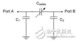
Figure 2 MEMS capacitor model
When the MEMS device design on the chip affects these parasitic capacitance values, C1 and C2 are not equal.
If the device is set to series, then the Cratio is usually 15. Note that there are also some grounded parallel parasitic capacitances present, and the value will depend on the capacitor size, typically 5-15% of Cmax.
However, if the device is set to a parallel state, such as Port B, one of the parasitic capacitors C1 is connected in parallel with the parallel digital capacitor, thus increasing the Cmin value. At this point, the Cratio is usually 7.
Quality factor (Q value)As for the Quality Factor part of the RF-MEMS capacitor, significantly reducing the metal beam resistance provides a key advantage: low loss. Such low wear is indicated by the "Q value" (quality factor) in the general specification. The Q value is actually the ratio of the reactive impedance (Xc) to the actual impedance (Rc), as shown in equation (2), where ESR is the "equivalent series resistance" of the capacitor.
Formula (2)
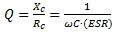
Decreasing the ESR of a particular C (capacitor) naturally increases the Q value. Metal traces on RF-MEMS beams provide very low ESR and are much lower than other technologies. The measured Q-value of RF-MEMS technology on a 1 GHz measurement wafer typically exceeds 200. In contrast, the Q value of a typical CMOS electronic device of the same frequency is typically less than 30.
LinearityThe linearity of the mobile RF front-end device is usually referred to as the Input Third-Order Intercept Point (IIP3). RF-MEMS devices are generally very linear, but are somewhat sensitive to the spacing of the dual frequencies. Two similar combinations of tones create a voltage envelope with a peak value of the sum of the voltages of each tone plus a low beat frequency variation between the two tonal differences. If the beat frequency is lower or closer to the mechanical resonance frequency of the RF-MEMS device, a higher degree of nonlinearity is measured. As mentioned above, mechanical resonance occurs in the 50-100 kHz range. Therefore, when the pitch is within this range, the IIP3 of the MEMS device is about +70 dBm; if the pitch is wider, the linearity can be increased to +80 dBm or more.
Also note that if the die is not properly grounded, modulation can occur between the RF traces on the MEMS device and the shielded CMOS circuitry. This modulation may increase the nonlinearity, so it is very important to ensure that the die is properly grounded.
Parameter index (FOM)To monitor and compare the most advanced tunable capacitors, the general Figure of Merit (FOM) is used here. This FOM can quickly evaluate all tunable capacitor technologies and measure their loss range, permittivity, power handling and cost (grain area).
Formula (3)
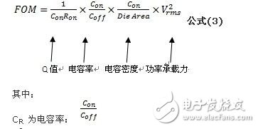
V2 is the RMS of the maximum voltage across the capacitor (Root-Mean-Square, rms)
Die Area is the required die area for the specified capacitor
Ron is the total series resistance in the on state
ReliabilityIn addition to the reliability conditions required for all semiconductor devices, this contact MEMS device has additional two types of reliability issues to be aware of:
• Stiction, a bond formed by two capacitive plates that cannot be loosened
• Wear-out, changing device characteristics due to long-term reuse
Adhesion is typically randomly occurring and can be controlled by the design of the MEMS device to avoid intimate contact between the metal and metal portions of the dielectric surface and/or high electric field portions. The best devices on the market today are carefully designed to prevent the drivers from touching each other, and the only area where contact occurs is the capacitor portion. It has therefore been determined that the sticking problem does not occur.
As for wear, it is a common factor in device failure and can be controlled by properly designing mechanical MEMS beams and contact areas. The complete product-level array contains dozens of RF-MEMS capacitive components that can operate continuously for more than 150 x 106 cycles, while one cycle refers to each customer's state change via the SPI or RFFE interface.
Voltage limitDrive by yourself
MEMS devices are driven by high-order DC voltages generated by integrated charge pumps. When this voltage is passed through the driver connector that is connected to the capacitor plate, the plates are pulled together by electrostatic force. This is the principle that the capacitor switches Cmax from Cmin.
The RF signal also changes voltage over time to form a voltage. This voltage oscillates at the RF frequency and is typically much higher than the self-resonant frequency of the MEMS device. Therefore, the RF voltage does not "directly" modulate the MEMS device. However, the device is driven by the square of the voltage that contains the DC and the second harmonic. This effective DC voltage is called the RMS (Root-Mean-Square Root Mean Square) voltage (see Figure 3). If the RMS voltage of the RF signal is too high, it will cause the MEMS device to "self-drive", thus causing the device to remain in a high capacitance state even if the program requires a low capacitance. To achieve such a high voltage at the front end of the mobile phone, high power is required, usually above 36 dBm, and high impedance resonance can occur in the filter or in some uncoordinated heights. Therefore, when the maximum RMS voltage of the RF passes through the driver terminal, a capacitor must be specified.
The relationship between power and voltage is shown in equation (4), where Z is the characteristic impedance of the system (usually 50 Ω) and Vpeak is the peak value of the RF voltage, as shown in Figure 3. The RMS voltage can be calculated using equation (5).
Formula (4)
![]()

Figure 3 Vrms is the DC voltage generated by the RF signal
(To use this graph, you also need to have a zero potential reference and Vpeak value)
Formula (5)

In a 50 Ω system, Vrms is
![]()
Driving it yourself will not cause damage to the device. Therefore, depending on the circuit configuration and the tolerance of the specification deviation, it is possible to generate the self-driving phenomenon described above again under the condition that the voltage is "absolutely maximum".
Thermal tuningThe RF-MEMS device will be closed due to the electrostatic force generated by the high voltage driver and will open as the drive voltage is removed. Once the electrostatic force disappears, the beam's elasticity will return the RF-MEMS device to the open state. For a variety of reasons, this spring force is usually less than the electrostatic force.
A lower recovery spring means that once the device is closed, it will only re-open when the drive voltage drops below the “release voltageâ€. The release voltage of the RF-MEMS capacitor is much lower than the drive voltage, which is only about 8V. It does not pose a problem under normal operating conditions because the integrated capacitor driver completely removes the drive voltage to open the capacitor.
If the RMS voltage in the RF signal passes through a MEMS capacitor and the voltage exceeds the release voltage, the driven MEMS device cannot be turned on. This limits the RF power that the capacitor can provide when switching to a low capacitance state. The power level at this time will again cause different degrees of problems (VSWR, voltage standing wave ratio) due to circuit configuration and load impedance, so unless the circuit configuration is known, the thermal tuning range must be based on RMS release. Voltage is set.
In a typical communication system, the tuner is typically reset during the pause of the data transfer stream. This is the so-called "compression mode" of WCDMA, or the general communication state of DTX. In addition, many systems that require thermal tuning operate at lower RMS voltages, so thermal tuning beyond the full power range is generally not required.
applicationFeed point tuner
Many commercial communication systems benefit from high performance tunable RF devices. The operating experience of both mobile phones and portable tablets is also limited by the antenna function. The size limitations make it difficult for antenna designers to design antennas that are compatible with each frequency band in a 50Ω device. At present, the mobile phone platforms are constantly increasing the frequency band, which makes the problem worse. Antenna designers are then forced to sacrifice the antenna's radiation efficiency to match the operating capabilities of each band.
Tunable RF devices can be used to create feed point tuners to optimize individual frequency bands for maximum radiation efficiency, not just 50Ω. This tuner will be able to adjust for each band operation to match the transceiver to the antenna load. Current WiSpry tuner products have an adjustment capability of over 19:1 VSWR and can span the 824 to 2170 MHz band using a dedicated wideband circuit configuration.
Currently, WiSpry tuner products are open-loop controlled. In this configuration state, a processor (usually a baseband processor, but not absolute) in the handset chipset of the industry standard digital bus format is used for control. As for the next generation of tuner products, closed-loop tuning applications, power sensors and feedback controllers will be added to the internal loop. In this way, the sensor also detects that the power is below the thermal tuning level and changes the configuration in time.
Antenna load tuner
The antenna load tuner can directly change the antenna resonance by directly adding the variable load to the antenna structure using a tunable RF-MEMS capacitor device, allowing the antenna to react to different changes depending on the tuning settings. This is another way to compromise radiation efficiency and multi-band compliance.
Tunable filter
Tunable RF devices can also be used in resonant circuit configurations and provide rejection or bandpass response at specific frequencies. These responses are all available for RF-MEMS capacitor regulation and provide a well-controlled digital tunable RF filter function.
Adjustable power amplifier
RF-MEMS devices can also be tuned to power amplifiers (PAs), which optimize the PA and adapt it to a variety of operating modes (linear and nonlinear), power levels and frequencies. Based on efficiency considerations, most commercial PAs use a traditional ladder network to match the output, and although the induction can only be achieved in a conventional, non-adjustable manner, RF-MEMS capacitors provide adjustable capacitive components.
to sum upThese advantages have brought many benefits to all aspects of the mobile phone industry. Operators can increase network bandwidth, increase availability and programmability of regional platforms with lower infrastructure costs, and have the opportunity to reduce customer churn through higher quality services and improved customer satisfaction. Mobile phone manufacturers can achieve performance gains of multiple dBs, reduce bill of materials (BOM), complexity, and make a smaller, thinner look, lower inventory (SKU), and get products to market quickly. Users can reduce the chance of missed calls, extend battery life by more than 35%, and buy more feature phones at a lower price, and talk instantly anytime, anywhere. Tunable RF with these advantages is expected to become the mainstay of LTE.
We are professional audio manufacturing company that makes a variety of speaker with bluetooth, including bluetooth portable speaker, bluetooth speakers outdoor, small speaker bluetooth, light bluetooth speakers, waterproof speakers etc.
With full turnkey service from product design to delivery, and every step in between.
From sophisticated custom audio systems to 'off-the-shelf' speaker drivers, iTopnoo has been saving our customers time, effort, and money.
To constantly offer clients more innovative products and better services is our consistent pursuit.
Best Portable Speakers,customizable bluetooth speaker, Custom jbl speakers, speaker wholesalers
TOPNOTCH INTERNATIONAL GROUP LIMITED , https://www.itopnoobluetoothes.com