Abstract: This application note describes how to configure Dallas Semiconductor's line interface unit (LIU) without adding a complicated microcontroller.
The configuration of LIU can configure the line interface unit (LIU) of Dallas without using a microcontroller. These unique LIUs have an additional serial interface (SPI) in addition to the traditional parallel interface. By floating some pins, pulling up to VCC or ground, the LIU can be configured in SPI slave mode. For specific pin configuration, please refer to the corresponding LIU data sheet.
Once the LIU is configured in serial mode, a PROM can be used to provide the required configuration data to the LIU. If the data in the PROM is stored in a defined format, the PROM works like a controller that provides an SPI host mode interface.
Usually this kind of PROM has an address accumulator inside. This accumulator function is very important for PROM, because PROM needs to automatically jump to the next valid address of the configuration memory. We recommend using Xilinx's XC18V00 series of byte-width nonvolatile memory with automatic address increment. This series of memory can provide 1Mb, 2Mb and 4Mb capacity.
Figure 1 shows the basic timing of the SPI bus. In this example, all data is sent to the slave synchronously on the rising edge of SCLK. This feature is configurable in some devices; for more details, you need to check the data sheet of the corresponding device.
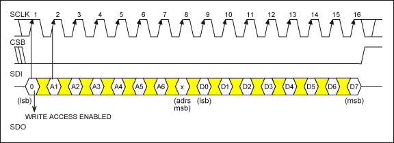
Figure 1. Serial interface timing for write operations
Figure 2 is a simplified connection diagram of Xilinx XC18V00 and Dallas working in SPI mode LIU. There are two points to note. The CLK of Xilinx XC18V00 can be MCLK of LIU, but the CLK is not the SCLK of SPI interface. SCLK can be set as required. Table 1 is an example of memory mapping. The setting of LIU starts when the OE of Xilinx XC18V00 becomes high. Therefore, it is necessary to consider whether a delay is required in the application. Usually connect the OE pin to the power-on delay device.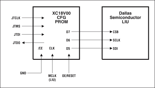
Figure 2. SPI and LIU connection.
Table 1. Memory configuration
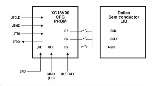
To configure LIU for other operations, connect the D5, D6 and D7 pins of Xilinx XC18V00 to the SDI pin of LIU through a switch, and use different loopbacks to implement other configurations of LIU.
The configuration of LIU can configure the line interface unit (LIU) of Dallas without using a microcontroller. These unique LIUs have an additional serial interface (SPI) in addition to the traditional parallel interface. By floating some pins, pulling up to VCC or ground, the LIU can be configured in SPI slave mode. For specific pin configuration, please refer to the corresponding LIU data sheet.
Once the LIU is configured in serial mode, a PROM can be used to provide the required configuration data to the LIU. If the data in the PROM is stored in a defined format, the PROM works like a controller that provides an SPI host mode interface.
Usually this kind of PROM has an address accumulator inside. This accumulator function is very important for PROM, because PROM needs to automatically jump to the next valid address of the configuration memory. We recommend using Xilinx's XC18V00 series of byte-width nonvolatile memory with automatic address increment. This series of memory can provide 1Mb, 2Mb and 4Mb capacity.
Figure 1 shows the basic timing of the SPI bus. In this example, all data is sent to the slave synchronously on the rising edge of SCLK. This feature is configurable in some devices; for more details, you need to check the data sheet of the corresponding device.

Figure 1. Serial interface timing for write operations
Figure 2 is a simplified connection diagram of Xilinx XC18V00 and Dallas working in SPI mode LIU. There are two points to note. The CLK of Xilinx XC18V00 can be MCLK of LIU, but the CLK is not the SCLK of SPI interface. SCLK can be set as required. Table 1 is an example of memory mapping. The setting of LIU starts when the OE of Xilinx XC18V00 becomes high. Therefore, it is necessary to consider whether a delay is required in the application. Usually connect the OE pin to the power-on delay device.

Figure 2. SPI and LIU connection.
Table 1. Memory configuration
| D7 | D6 | D5 | D4 | D3 | D2 | D1 | D0 | |
| Address | CSB | SCLK | SDI | X | X | X | X | X |
| 0x00 | 1 | 0 | 0 | Start of Write Cycle | ||||
| 0x01 | 0 | 0 | 0 | Bit A0 (Always a "0" for a write) | ||||
| 0x02 | 0 | 1 | 0 | |||||
| 0x03 | 0 | 0 | 1 | Bit A1 | ||||
| 0x04 | 0 | 1 | 1 | |||||
| 0x05 | 0 | 0 | 0 | Bit A2 | ||||
| 0x06 | 0 | 1 | 0 | |||||
| 0x07 | 0 | 0 | 0 | Bit A3 | ||||
| 0x08 | 0 | 1 | 0 | |||||
| 0x09 | 0 | 0 | 0 | Bit A4 | ||||
| 0x0A | 0 | 1 | 0 | |||||
| 0x0B | 0 | 0 | 0 | Bit A5 | ||||
| 0x0C | 0 | 1 | 0 | |||||
| 0x0D | 0 | 0 | 0 | Bit A6 | ||||
| 0x0E | 0 | 1 | 0 | |||||
| 0x0F | 0 | 0 | 0 | Bit A7 | ||||
| 0x10 | 0 | 1 | 0 | |||||
| 0x11 | 0 | 0 | 0 | Bit D0 (LSB) | ||||
| 0x12 | 0 | 1 | 0 | |||||
| 0x13 | 0 | 0 | 1 | Bit D1 | ||||
| 0x14 | 0 | 1 | 1 | |||||
| 0x15 | 0 | 0 | 1 | Bit D2 | ||||
| 0x16 | 0 | 1 | 1 | |||||
| 0x17 | 0 | 0 | 0 | Bit D3 | ||||
| 0x18 | 0 | 1 | 0 | |||||
| 0x19 | 0 | 0 | 0 | Bit D4 | ||||
| 0x1A | 0 | 1 | 0 | |||||
| 0x1B | 0 | 0 | 1 | Bit D5 | ||||
| 0x1C | 0 | 1 | 1 | |||||
| 0x1D | 0 | 0 | 1 | Bit D6 | ||||
| 0x1E | 0 | 1 | 1 | |||||
| 0x1F | 0 | 0 | 0 | Bit D7 | ||||
| 0x20 | 0 | 1 | 0 | |||||
| 0x21 | 1 | 0 | X | End of Write Cycle | ||||
| 0x22 | 1 | X | X | |||||

Portable high efficient travel charger, can charge multi devices at the same time, every port output mini 5v 1a, max 5v 2.1a. We can meet your specific requirement of the products, like label design. The plug type is US/UK/AU/EU. The material of this product is PC+ABS. All condition of our product is 100% brand new.
Our products built with input/output overvoltage protection, input/output overcurrent protection, over temperature protection, over power protection and short circuit protection. You can send more details of this product, so that we can offer best service to you!
Usb Charger,Universal Travel Adapter,Intelligent Usb Charger,Travel Adapter
Shenzhen Waweis Technology Co., Ltd. , https://www.szwaweischarger.com