1 Introduction
This article refers to the address: http://
In the past ten years, high-definition digital television (HDTV) services have been widely promoted and applied around the world (the United States first opened the road-based cable network of HDTV in 2003, and China has also determined that HDTV will gradually replace the traditional TV network in a few years), but Because of the huge amount of video data, it is not convenient to store and transmit. However, the traditional compression system has the characteristics of low compression quality and low real-time performance. Therefore, it is of great significance to study the compression system based on high-definition video signals. ADV 212, a new codec chip from AD Company of the United States, uses wavelet transform and adaptive arithmetic coding technology, with layered transmission, focus area compression, multi-scale, multi-resolution analysis and time domain localization. The signal can be easily transmitted to the central console via wired or even narrowband wireless channels, with the advantages of large compression range and high compression quality. Therefore, this paper designs an efficient video compression system combining ADV212 with FPGA and DSP.
2 ADV212 structure and function
2. 1 internal structure
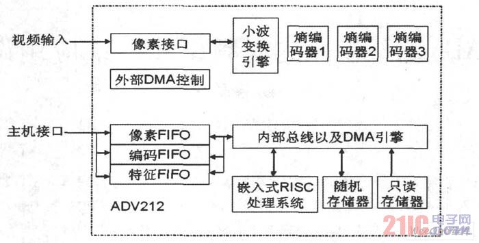
The ADV212 is a low cost, monolithic, low power, all digital CMOS VLSI. It achieves the high-intensity calculations necessary for JPEG2000 image compression while producing a code stream for most applications. The chip's core operating voltage is 1. 5V, I /O voltage 2. 5V to 3. 3V, mainly includes a specialized wavelet transform engine, 3 entropy encoders, an on-chip memory, and a built-in reduced instruction set (R ISC) )processor. The image or video data is input by the AD internal 12-bit pixel interface. The sampled result is interlaced into the wavelet transform engine, and then each block or frame is decomposed into sub-bands using a 5 / 3 or 9 / 7 filter, and the obtained wavelet coefficients are written. Internal memory. The entropy codec encodes the data into the JPEG2000 standard. The internal DMA engine provides high bandwidth transfers between memories and high performance transfers between modules and memory. Figure 1 shows the internal function of the ADV212.

Figure 1 Internal functional structure diagram of ADV212
2. 2 ADV212 function module analysis
(1) Wavelet transform engine.
The DV212 provides a high-precision wavelet transform processor that enables 6-level wavelet decomposition. In the coding mode, the wavelet processor transforms and quantizes the original sampled data, and stores the wavelet coefficients in the internal memory.
In the decoding mode, the wavelet transform coefficients are read from the internal memory, and the original data before encoding is obtained by decoding calculation.
(2) Entropy encoder.
The entropy codec is used to perform background modeling and arithmetic coding on the coded blocks of wavelet coefficients, and at the same time to calculate the distortion necessary for optimal rate and distortion performance in the compression process. Since the entropy encoding process has the highest computational requirements in the JPEG2000 compression project, the ADV202 internally provides three dedicated hardware entropy codecs.
(3) Internal memory.
The main functions of the storage system are to manage wavelet coefficient data and temporary code block feature data, as well as to create, decompose, and store temporary workspaces for JPEG2000 code streams. In addition, the storage system is also used for program and data storage of the R ISC processor.
(4) Embedded R ISC processor.
The ADV212 embeds a 32-bit R ISC processor that can be used to configure, control, and manage other dedicated hardware blocks and to decompose and generate JPEG2000 video streams. The RISC processor has ROM and RAM corresponding to each program and data memory, interrupt controller, standard bus interface, and timer counter.
2. 3 main features
A single JPEG2000 compression and decompression solution for video and still images.
Consistent with the chip ADV202 pin, it supports all the functions of the ADV 202.
New support for JTAG /boundary scanning is added, and power consumption is 30% lower than ADV 202.
Low-power and low-cost beamlet compression with unique spatially efficient regression filtering (SURF) technology, supporting up to 6 levels of 9/7 and 5/3 wavelet conversion.
Use 5 / 3 wavelet programmable block / image size in 3 component 4: 2: 2 interlaced scanning width up to 2048 pixels, single compression mode up to 4096 pixels, maximum tile / image height 4096 pixels.
Supports various video interface protocols such as ITU-R B. T656, SMPTE 125M PAL /NTSC, SMPTE 274M, SMPTE 293M ( 525p ), ITU - RBT. 1358 ( 625p), and irreversible mode maximum input speed of 65M sps, reversible mode Any video format with a maximum input speed of 40Msps.
Two or more ADVs 212 can be combined with full frame SMPTE274M HDTV (1080i) or SMPTE 296M (720p).
The SD video source frame can be temporarily interlaced to improve quality.
The flexible asynchronous SRAM type main interface seamlessly connects to 16/32-bit microcontrollers and ASICs.
2. 4 ADV 212 software configuration
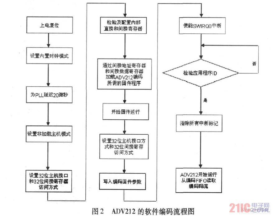
The operating mode of the ADV212 is set by writing the status word of the register in the initialization firmware. The firmware program has the suffix name *. sea, which is downloaded to the indirect memory of the ADV212 via the USB interface. The address segment is 0x00050000~ 0x0005EFF, data width. 32b its. The encoding process of the ADV212 program using C language is shown in Figure 2.

3 HD video compression system design based on ADV212 chip
The system is based on the ADV212 and is equipped with a general-purpose processor to achieve high-definition video signal compression with a resolution of 1080 μ.
3. 1 multi-chip encoding mode
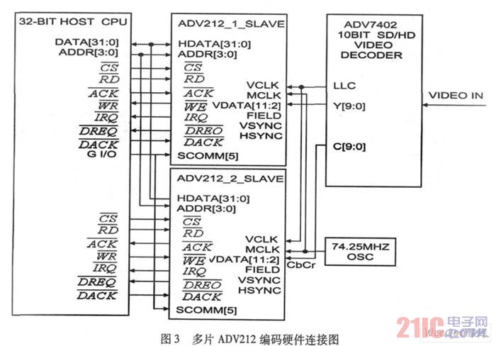
Since the ADV212 has a maximum data input rate of 65 Mbps and 40 Mbps in irreversible and reversible modes, and an effective video conversion input data rate of approximately 124 Mbps, at least two ADVs 212 are required to implement full resolution 1080 i video signals. decoding. In the encoding process, Y data and CbCr data are input to the ADV 212 through different buses, wherein AD212_1 processes the luminance data of the 1080i video signal, and ADV202_2 is used to process the chrominance data of the 1080i video signal. In order to synchronize the corresponding output data in this application mode, the input data must be in the EAV / SAV encoding format. For higher performance, such as lossless compression of 1080i video, 3 or more ADVs 212 can be used to process the signal. Figure 3 shows the hardware connection diagram of two ADV212 codes.

When multi-chip mode of ADV 212 is encoded, the chip is usually used as a slave device, and can be divided into master/slave or slave/slave mode at the time of decoding. In master-slave mode, the HVF output of the master is connected to the HVF input of the slave, and the SCOMM of the master slave is also connected to the same IO pin of the controller. In Slave mode, the HVF of ADC212 is generated by the same external sync signal and SCOMM is connected to the same IO pin of the controller. In multi-chip mode, SW IRQ1 of all ADV 212 is not masked and SW IRQ 1 is in the E IRQ IE (External Interrupt Enable) register.
3. 2 system design
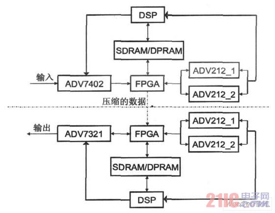
Based on the multi-chip connection mode and high-efficiency compression performance of the ADV212 chip, combined with the programmability of FPGA + DSP, we designed a video compression system as shown in Figure 4. As can be seen from the figure, the system is mainly composed of A/D converter, FPGA module, DSP module and ADV212 encoder/decoder. The functions and technical approaches of each part are as follows:
The A/D conversion is done by the ADV7402, which automatically detects and converts standard analog baseband TV signals into CC IR656's 4:2: 2 component digital video data. The D/A conversion at decompression is done by the ADV7321.

Figure 4 System structure block diagram.
As the backbone of the entire system, the FPGA module bridges the signals of the various chips in the system. First, the initial processing of the image data (such as denoising) is completed as needed, and then the data is divided into two sub-blocks of the same size so that they can be processed in the two ADVs 212, respectively.
At the same time, it is necessary to provide reset, chip select, line sync, read and write, and clock signals to the ADV212 to control the working timing and working mode of the ADV212, and provide a reset signal for the DSP. During the work process, the FPGA continuously sends feedback information about the working status to the outside. After receiving the external transmit! command, the code stream will be fetched from the memory, which the FPGA converts into a bitstream format and sends it to the channel.
The DSP module is the master of the system, which completes the initialization of the ADV 212 and ADV7402. The JPEG2000 format code stream generated by the ADV212 is first sent to the DSP for encryption, and then stored in the SDRAM for reception! The transmission command is sent by the DSP to the code stream to be transmitted stored in the SDRAM after receiving the ! /String converts the DPRAM and finally converts it into a serial bit stream in the FPGA for transmission.
After the system starts working, an external analog video signal is transmitted to the ADV 7402. The ADV7402 is sampled and quantized to output the required digital video data. The video data stream is relayed to the ADV 212 via the bridge of the FPGA. In order to increase the compression ratio, the data stream can be lost when the video data stream flows through the FPGA, so as to artificially reduce the source data rate that needs to be compression-encoded.
The compressed data is then transmitted by the ADV 212 to the interface controller in the FPGA, and the controller outputs the compressed data stream according to the specified interface protocol.
4 Conclusion
Combining the high flexibility of FPGA and DSP, using the multi-chip mode of ADV 212 and efficient compression, a compression/decompression system is designed to solve the problem of high compression and high quality of HD video signals. The launch and popularization of digital TV services have laid a good foundation.
CSRME safety controller is developed for standard GB27607. By monitoring machine tool safety related equipment, the security of machine control system can meet the requirements of GB27607, and its security meets the requirements of ISO13849-1 (PLe) and IEC61508 (SIL3).
With rich interfaces, CSRME has limited programmable function. It can simultaneously replace many different types of safety control modules or safety PLCs, thus greatly simplifying the safety design of machine control systems and reducing cost.
Safety Controller,Modular Safety Controller,Safety Controller,Electrical Safety Controller,Programmable Logic Controller,Banner Safety Controller
Jining KeLi Photoelectronic Industrial Co.,Ltd , https://www.sdkelien.com