As with any design decision , there are several variables to consider when choosing the right MOSFET driver for your design's MOSFETs . The parameters to be considered need to include at least input-to-output transmission delay, quiescent current, anti-blocking, and current drive capability. The power consumption of the driver also affects the decision of the package and the choice of driver. This application note will discuss in detail the MOSFET driver power dissipation associated with MOSFET gate charge and operating frequency . Also discuss how the on and off time of the current driving capability of the MOSFET driver MOSFET gate charge required to match a MOSFET according to. Microchip offers many different types of MOSFET drivers in different packages that allow designers to choose the most suitable MOSFET driver for the MOS-FET in an application .
Power consumption of MOSFET driver
The same amount of energy is required to charge and discharge the MOSFET gate regardless of whether the charge or discharge process is fast or slow (gate voltage rise and fall). Therefore, the current drive capability of the MOSFET driver does not affect the power dissipation of the driver due to the capacitive loading of the MOS-FET gate.
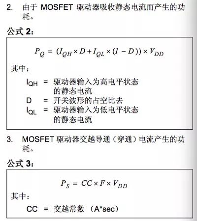
The power consumption of a MOSFET driver consists of three parts: 1. Power consumption due to charge and discharge of the MOSFET gate capacitance.
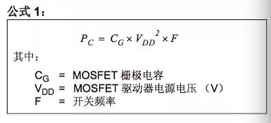
Derive from the above formula, only one of the three parts of power consumption is related to charging and discharging of MOSFET gate capacitance. This part of the power consumption is usually the highest, especially at a very low switching frequency.
To calculate the value of Equation 1 , you need to know the MOSFET gate capacitance.
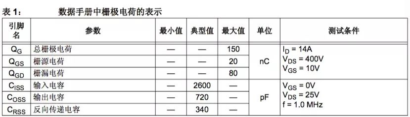
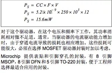
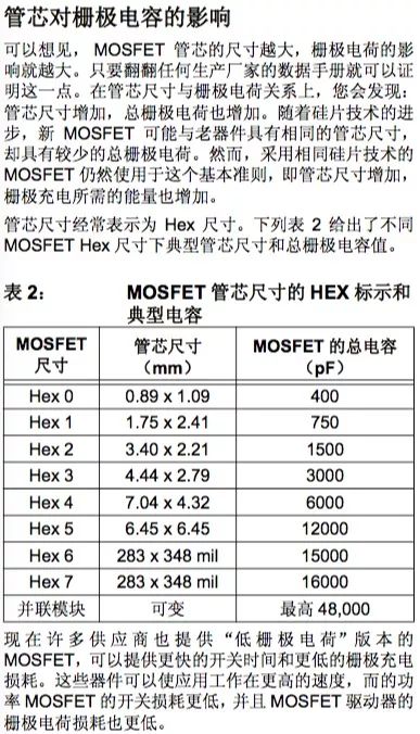
The MOSFET gate capacitance contains two capacitances: gate-source capacitance and gate-drain capacitance (Miller capacitance). The common mistake is to use the MOSFET 's input capacitance ( C ISS ) as the MOSFET's total gate capacitance. Determine the correct method is to look at the total capacitance of the gate capacitance of the gate (Q G) MOSFET data sheet. This information is usually displayed in the electrical characteristics of any MOSFET
Sex table and typical characteristic curve.
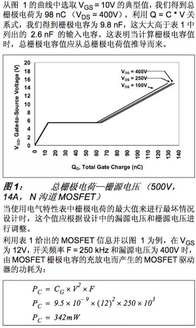
Table 1 shows a typical example of the gate capacitance for 500V , 14A , N- Channel MOSFETs in the data sheet. It is important to note that the values ​​given in the data sheet table relate to their test conditions: gate voltage and drain voltage. These test conditions affect the value of the gate charge. Figure 1 shows the typical characteristics of the gate charge for the same MOSFET at different gate and drain voltages. Make sure that the value of the gate charge used to calculate the power consumption also satisfies the application conditions.
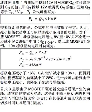
The crossover turn-on characteristic is shown in the MOSFET driver data sheet as the "crossover energy - supply voltage" typical characteristic curve. Figure 2 shows an example of this curve.
The unit of constant constant is usually amp - second ( A*sec ). This value is multiplied by the operating frequency to obtain the average current value. Figure 2 demonstrates this previously discussed. That is, as the bias voltage increases, the crossover constant also increases, so the driver's power consumption (due to cross conduction) also increases. Conversely, reducing the driver voltage causes the driver power consumption to decrease.
One thing to note is that when using two-way drivers, the crossover constant usually indicates the operation of the two parts of the drive. If only a portion of the drive is used, or if the two parts of the drive are operating at different frequencies, only half of this value needs to be used for the calculation of each part of the drive.Taking the information shown in Figure 2 as an example, we assume that this is a single output driver with a working V DD of 12V and an operating frequency of 250 kHz . Based on the above curve, the crossover constant is set at 5.2*10 -9 .
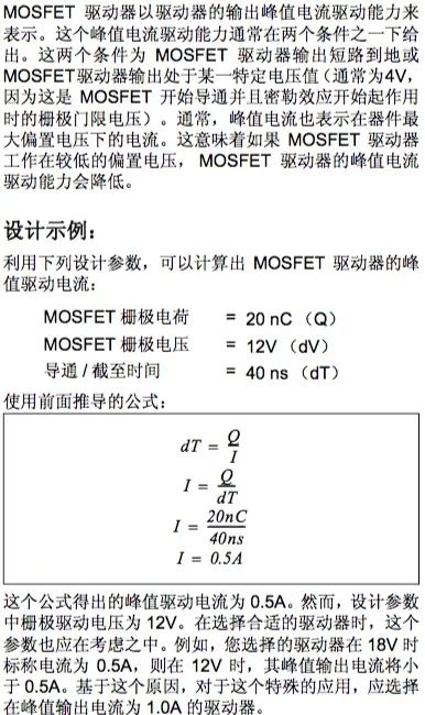
Peak Current Drive Requirements
The discussion for MOSFET drivers is mainly to consider the internal and external factors that cause the MOSFET driver to generate power. Therefore, it is necessary to calculate the power loss of the MOSFET driver and use the calculated value to select the correct package and calculate the junction temperature for the driver.
Matching the MOSFET driver to the MOSFET in the application is mainly based on the speed of the power MOSFET turning on and off (gate voltage rise and fall times). The optimum rise/fall times for any application depend on many factors such as EMI (conduction and radiation), switching losses, inductive reactance of the pin/circuit, and switching frequency.
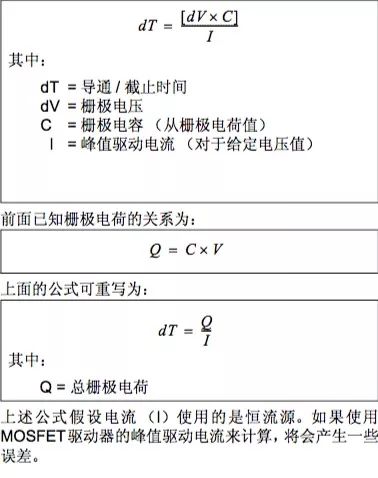
The speed at which MOSFETs turn on and off depends on the charging and discharging speed of the MOSFET gate capacitance. The relationship between MOSFET gate capacitance, turn-on and turn-off times, and the drive current of the MOSFET driver can be expressed as:
Also consider using an external resistor between the MOSFET driver and the power MOSFET gate as this will reduce the peak charge current that drives the gate capacitance. This drive configuration is shown in Figure 4 .
MOSFET Driver Gate Drive Typical Configuration
Many different circuit configurations can be used when using MOSFET drivers. In many cases, additional clamping circuits need to be considered due to high peak currents, fast rise/fall times of the drive voltage, and inductance due to long traces on the board. Figures 3 to 6 show typical configurations of gate drive circuits that are often used.
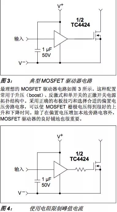
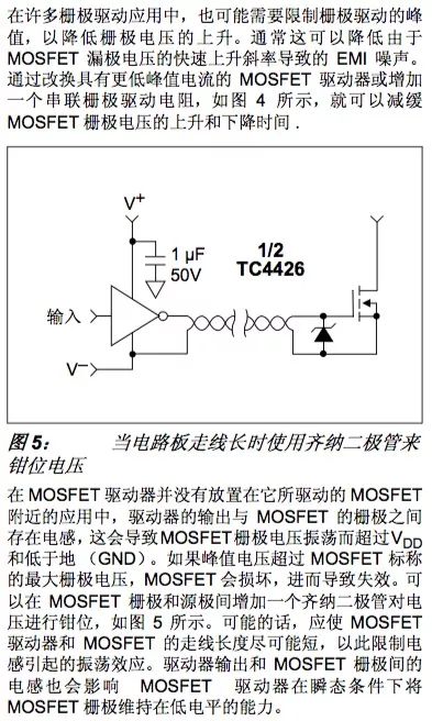
Figure 6 shows two different gate drive configurations using a gate drive transformer. Gate drive transformers can be used in high voltage or low voltage applications to provide isolation between the control circuit and power MOSFETs , either to meet safety requirements or to provide high-side floating gate drivers.
Circuit A and Circuit B in Figure 6 show gate drive transformers used in single-switch forward applications. The resistors and capacitors in series with the MOSFET driver output and gate drive transformer are used to balance the voltage - time of the gate drive transformer . Since the voltage - time of the gate drive transformer must be balanced (the same for any transformer), a negative gate-to-source voltage is applied to the gate of the power MOSFET during the off-time of the switching cycle . Many times this can cause switching time delays at turn-on. If you do not want this to happen, you can use the circuit configuration in B. This circuit uses a negative gate drive voltage to turn on another small-signal FET , which in turn shorts the gate and source terminals of the main power MOSFET , completely turning it off and keeping the gate voltage at 0V . The drive configurations shown in A and B can also be used for the dual-switch forward topology.

to sum up
In practical applications, many parameters need to be considered when matching an appropriate MOSFET driver to a MOSFET . However, the correct choice can be made by following the steps described in this application note. Table 3 can be used as a general guide to narrow the selection.
Just like any electronic component, no single device can fit all applications, so Microchip offers MOSFET drivers with different nominal currents, drive output polarity, and input logic configuration .
More stable performance
Disposable ecig have a completely enclosed design, reducing the need for charging and replacing cartridges. The no-charge design also reduces the occurrence of faults. It is understood that with rechargeable e-cigarettes, each cartridge needs to be charged at least once and the battery efficiency is extremely low, while the design of disposable ecig can solve this problem very well.Disposable ecig are very easy to carry on daily trips, no need for any operation in the use of airflow induction, direct suction can be out of smoke, meaning that you just need to suck directly on the hand can be the main feature of the small cigarette is practical portability is the main, its appearance is very small, no longer like the previous big smoke box mechanical rod nowhere to put.
The market outlook for disposable ecig
There has been a controversial topic regarding the use of disposable ecig. According to scientific studies, the long-term use of e-cigarettes can cause harm to the human body, no less than tobacco. Therefore, it is important not to overuse either type of e-cigarette - after all, smoking is bad for your health. Specifically, the PMTA requires that any new tobacco product be approved by the FDA for legal promotion and that the FDA consider all aspects of the product to be beneficial to public health. Our products can always be sold under the supervision of the PMTA at cost and are prohibited for sale to minors. We have strict guarantees regarding the quality of our products.
Disposable E-Cig,Disposable Vape Pen Oem,Best Disposable Vapes,One-Time Use Vape
Shenzhen MASON VAP Technology Co., Ltd. , https://www.disposablevapepenfactory.com