IR2103 is a half-bridge driver integrated chip. It integrates independent control drive output circuits and can directly drive two medium power semiconductor devices such as MOSFET or IGBT. It has fast dynamic response, strong driving capability and high operating frequency. With a variety of protection features. The IR2103 is equipped with a large pulse current buffer stage to minimize cross-conduction and a Schmitt-triggered input design with pull-down to effectively isolate noise to prevent accidental turn-on of the device.
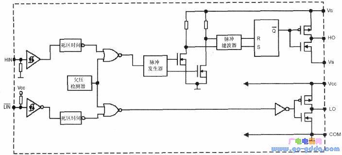
The block diagram of the IR2103 chip is shown in the figure above. The pin functions are as follows:
1 pin VCC: logic power supply and low-end power supply voltage;
2 pin HIN: high-end logic input;
3-pin LIN: low-side logic input;
4-pin COM: low-end power supply grounding;
5-pin LO: low-side drive output voltage;
6-pin Vs: high-side floating power supply reference voltage;
7 feet HO: high-end drive output voltage;
8-pin VB: High-side floating supply voltage.
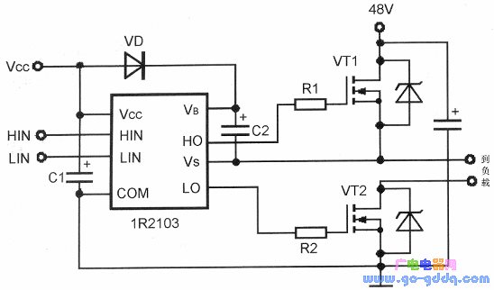
The typical wiring of IR2103 is shown in the figure above. In the figure, VCC is a 10~25V power tube gate driver. TTL or CMOS logic signals can be used as input. Therefore, VCC can use a power supply with a typical value of +15V. C2 is the bootstrap capacitor. When VT1 is turned off and VT2 is turned on, VCC charges C2 via VD, C2, load, and VT2 to ensure that VT2 is turned off and VT1 is turned on. Drive to achieve bootstrap driving. If the load impedance is large, C2 is slower to charge through the load, so that when VT2 is turned off and VT1 is turned on, the voltage on C2 cannot be charged until the bootstrap voltage is 8.2V or higher. The output drive signal will be on-chip due to undervoltage. With logical blocking, VT1 will not work properly. Each cycle of VT2 is switched once, and C2 is charged once by switch VT2. Therefore, the capacity selection of C2 should consider the following points:
(1) C2 should be high-stability, low-series inductance, high-frequency characteristics of high-quality capacitors, capacity is 0.1~10μF; (2) try to make the bootstrap power-up loop without large impedance load, otherwise it should provide fast charging for C2 charging path:
(3) When the PWM switching frequency is high, C2 should be selected small.
When the PWM operating frequency is low, if the duty cycle is higher, the VT1 turn-on time is longer, the VT2 turn-on time is shorter, so C2 should be selected smaller; if the duty cycle is lower, VT1 turn-on pulse width is narrower, then VT2 lead The pass pulse width is wider and the bootstrap voltage is easy to satisfy. Otherwise, the bootstrap voltage cannot be reached for a limited time, causing the undervoltage protection circuit to work. Therefore, the choice of C2 should take into account the various conditions of PWM changes, it is best to monitor the waveforms of the HO and VS feet during debugging.
The working principle of IR2103 is very simple. When the bootstrap is satisfied, when the 2-pin HIN high-side logic input of IR2103 is high level, the 7-pin HO high-side drive output voltage terminal outputs a high level, which makes the upper bridge VT1 turn on. When the 3-pin LIN low-side logic input of IR2103 is high, the 5-pin LO low-side drive output voltage terminal outputs a high level, which turns the lower bridge VT2 on. Due to the dead time control, the 5-pin LO low-end drive output voltage and the 7-pin HO high-end drive output voltage will not appear high at the same time. That is, the upper and lower bridges VT1 and VT2 will not be turned on at the same time, that is, There is no straight-through phenomenon.
The 2 and 3 pins of the IR2103 are controlled by the microcontroller. In the brushless motor control circuit of the electric bicycle, the three IR2103s are controlled by the single chip microcomputer. For the three-phase bridge inverter composed of six power components, the three bridge arms are driven by three IR2103s. Ideal for power conversion. The main circuit in such an inverter circuit can invert the DC voltage (+VCC) into a three-phase AC output voltage U, V, W, and send it to the brushless motor. Since the three-phase inverter always has one upper and lower tube conducting every cycle, the bootstrap capacitor of the upper tube is easy to be charged, and the three upper tube bootstrap circuits can work in an orderly manner. However, if the IR2103 is used improperly, especially if the bootstrap capacitor is not properly selected, it may cause the chip to be damaged or not working properly.
SHENZHEN CHONDEKUAI TECHNOLOGY CO.LTD , https://www.szfourinone.com