The control terminal is an indispensable main component of the measurement and control device, and it is the basis of the existence of the measurement and control system. Many of the measurement and control systems currently applied have large scale, scattered control points, low computational density of most control points, and a wide variety of controlled bodies and interfaces. Features.
In recent years, embedded systems are suitable for calculating low-density distributions due to their small size, low power consumption, strong control functions, ability to embed an operating system, and easy expansion of peripheral interfaces (including various fieldbuses and hundreds of megabytes). Control the application of the terminal. This design uses ARM9 3C2440 to develop the measurement and control terminal, and completes RS485, RS232, CAN, IO input/output and IIC communication control interface design in the measurement and control device. The following focuses on its design methods and processes.
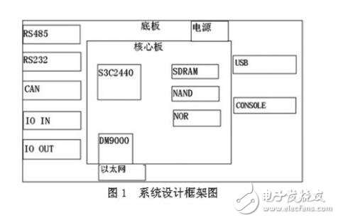
1 system designThe overall structure of the system of Figure 1 is the structure of the core board and the bottom board. The core board's resources include the S3C2440A's ARM920T core-based processor, which integrates a number of peripherals that can be easily extended to form a variety of control/communication interfaces. The storage system has 64M SDRAM, 256M NAND FLASH, and 2M NOR FLASH on the core board to meet the general industrial control needs. In addition, the DM9000 Ethernet control chip is integrated on the core board. On the backplane, the function modules on the S3C2440 processor are added, together with the peripheral circuits, to form various interface extensions, including half-duplex RS485, RS232, CAN communication modules, IO digital port input, and IO port digital Output.
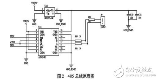
S3C2440 integrated three-way UART interface, UART interface can be easily converted to 485 interface through level conversion chip. UARTO is used as the console (conso le) interface for embedded LINUX, UART1 is used as RS485 extension, and UART2 is used as RS232 extension. We are using UART1. Since the pin level of the ARM processor is different from the electrical standard specified by the EIA, an external level conversion chip must be used. The RS485 or RS232 serial protocol standard can be easily implemented by using an on-chip UART externally connected to different conversion chips. RS485 uses differential signal negative logic. In order to meet the electrical characteristics of the RS485 bus, Analog Devices' half-duplex RS-485 isolated transceiver is used in the design.
The ADM2483 is an isolated enhanced RS485 transceiver that includes a three-channel isolator, a differential driver with a three-state output, and a differential receiver with a three-state input that allows up to 256 transceivers to be connected to the bus. The transmission rate is 500kb/s, and the logic terminal is compatible with 3V/5V working power. The bus terminal is powered by 5V.
Figure 2 is a schematic diagram of a half-duplex RS-485 bus using the ART1 in the S3C2440. The pins RE' and DE are the receive enable and transmit enable terminals respectively. Now connect them in parallel to the S3C2440. The nCTS0 pin, the level of the pin controls the direction of the chip data. To send a data, set it to 1 and clear it to 0 when receiving data.
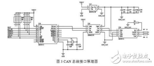
The MCP2515 is a stand-alone controller local area network protocol controller that fully supports the CAN V2.0B specification. The device can send and receive standard and extended data frames as well as remote frames. The MCP2515's two acceptance mask registers and six acceptance filter registers filter out unwanted messages, thus reducing the overhead of the host microcontroller. The MCP2515 is connected to the MCU via an industry standard Serial Peripheral Interface (SPI). On the S3C2440 processor, two SPI controllers are integrated on-chip, which can be connected to the control line of the MCP2515 through the SPI bus, and then control and configure the MCP2515. In addition, to form a CAN network, a CAN transceiver connected to a specific physical line is still needed. In this design, Microchip's MCP2551 is used. The MCP2551 is a fault-tolerant high-speed CAN device that acts as an interface between the CAN protocol controller and the physical line. It functions as a differential transceiver for the CAN controller and converts the digital signals generated by the CAN controller into signals suitable for transmission over the bus. .
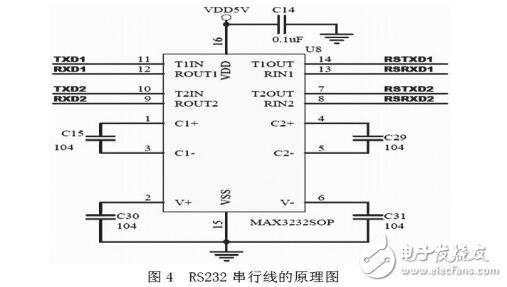
RS232 is suitable for communication between local devices. Serial data can be easily transferred using the S3C2440's on-chip UART. The MAX232 operates from a single voltage of 5V, making it easy to level shift, especially without a 12V supply. The chip is packaged in a DIP and integrates two voltage converters for easy and convenient wiring.
The digital input and output can directly control the ARM pin to achieve the GPIO function, and the input and output have the same principle. The general control system needs to work in a harsh environment, the voltage value will be abrupt, and generally higher than the acceptable range of the ARM processor, so some isolation measures must be taken, and an external isolation chip is required. The isolation chip plays three roles in the circuit: 1) isolating the breakdown voltage and preventing the processor from being damaged; 2) completing the logic level conversion, converting the logic level of the signal in the industrial control to the embedded processing The logic level allowed by the device; 3) isolating noise and suppressing common mode signals. The ADI's ADuM1200 digital isolator is used in this design. This digital isolator uses iCoupler magnetic isolation technology, which has the advantages that traditional opto-isolators can't match in terms of performance and work volume. It has higher data transmission rate and timing precision than optocoupler. Transient common mode rejection. Two independent isolation channels are integrated on one chip, and the working voltage is 2.7V~5.5V at both ends. Each isolation channel has low pulse width distortion and DC correction function. Combining the above advantages is the reason for adopting the isolation chip in this design.

The design is successfully applied in the environmental measurement system of the neutrino laboratory, which realizes the embedded operating system, network interconnection function, miniaturization and high reliability design of the industrial site, and the operation is stable and reliable, and the effect is good. However, there is a defect that the speed is not high in long-distance communication, and the specific solution needs further study.
include Coin Deposit Module and Banknote Deposit Module
banknote deposit module coin deposit module support OEM
Suzhou Ribao Technology Co. Ltd. , https://www.ribaoeurope.com