- Model NO.: Mouse Pad
- Feature: Non-Heated
- Type: Photo Mousepad
- Wrist Rest: Without Wrist Rest
- Product Name: Rubber Eprgonomic Round Mouse Mat for Gifts
- Size: 20*20*0.3cm or Customized Size
- Logo: Customzied Logo
- Characteristic: Non Slip, Precise Positioning
- Certifcation: BV, Reach, RoHS, Azo Free and Other Chemical Tests
- Transport Package: 1 Pair in OPP Bag
- Origin: Jiangsu, China (Mainland)
- Material: Fabric
- Applications: Game
- Side Number: Single Sided
- Color: Customized Color
- Printing: Heat Tranfer Printing
- Thickness: 1mm,2mm,3mm,etc.
- Usage: Office, Home, Games
- Customized Sample: Available for Free
- Trademark: EAST SUNSHINE
- Specification: Microfiber, Natural rubber
- HS Code: 4016999000
Â
| Specification | |
| Material | Microfiber,Natural rubber |
| Color | Customized Color |
| Size | 20*20*0.3cm or Customized Size |
| Thickness | 1mm,2mm,3mm,etc. |
| Logo Printing | Heat Transfer Printing,customized Logo |
| Characteristic | Non slip, precise positioning |
| MOQ | 500 |
| Lead Time | 7-15days for MOQ |
| Payment | T/T, West Union, PayPal, and so on |
Our Advantages
1.Natural Material
Our mouse pad is mainly used natural foam rubber, small bubbles anddense, so that the mouse is flexible and elastic, thick design, the operation feel more comfortable.
2.Soft and Comfortable Fabric with Fine Lines
Fine cloth, mouse operation process more smoothly, use for a long time without heating, Matt fine textured, with higher precision tracking, effectively reduce the long time using the mouse caused by hand fatigue.
3.HD printing process
The use of high-definition printing technology production, do not fade, vivid, fresh
4.Mouse Mat Non Slip Bottom
The bottom of use rubber material, safe non-toxic tasteless, super adhesion lines firmly attached to the desktop, non slip solid.
5.Precision Sewing
Sewing mouse pad edge by knitting method particularly fine, can remove the redundant edges to ensure continued, mouse pad is more durable.
Â
| Packing and shipping | |
| Packing | 1 Pair in OPP Bag, 240 pcs in one carton |
| Standard Carton Size | 48*39*39cm |
| Gross Weight per Roll | 24.8kg |
| Customized packing | Customized packing is also acceptable |
| Shipping options | |
| Less than 100kg:By international enpress,door to door service,short of shipping duration. | |
| More than 100kg:By ocean or air,easy to handle | |
| According to customer's instruction. | |
FAQ
1.Why Choose Us?
A) Quick Reply:We will reply your inquiry within 24 hours.
B) Factory:We have our factory.We will provide you better price with fair quality.
2.How do we deal with different customers?
A) For professional buyer:We will serve you with our professional sales manager and offer you best solution under you detailed inquiry.
B) For those who buy only several times:We will offer you best design and production plan to fulfill your demand.
3.How to contact us?
A) Directly contact us in Alibaba.Our sales managers will answer your inquiry from Alibaba within 24 hours.
4.I only want to buy small order for testing.Is that OK?
A) Small order is acceptable.We will offer such inquiry by using the stocked cloth.
5.Can IÂ get samples first before we give order?
A) Yes, free samples are offered.We will first make drawing according to your design, and then we will make free sample to you.
B) Mould fee and shipping fee will not be included.
6.When can IÂ get the sample or my order?
A) Samples are to be finished in 2Â or 3Â days.
B) Mass production will take 7Â to 10 days for MOQ quantity.
Negotiation process
Enquiries =>Offer=>Counter offer=>Sign a contract=>Shipping=>Take goods=>Feedback
HDI PCB or High density interconnect PCBs are a way of making more room on your printed circuit board to make them more efficient and allow for faster transmission. It's relatively easy for most enterprising companies that are using printed circuit boards to see how this can benefit them.
High density interconnect (HDI) PCBs represent one of the fastest-growing segments of the printed circuit board market. Because of its higher circuitry density, the HDI PCB design can incorporate finer lines and spaces, smaller vias and capture pads, and higher connection pad densities. A high-density PCB features blind and buried vias and often contains microvias that are .006 in diameter or even less.
The copper is the circuits material and the circuits designed by the PCB designers. Depends on the current in the circuits, the PCB copper thickness could be done with 0.5oz-10oz. But the PCB designers need be noted that the copper track width/space need be enlarged with the thickness. For example, the minimum copper track width/space could be 3mil/3mil with 0.5oz, but would be 4mil/4mil with 1oz.
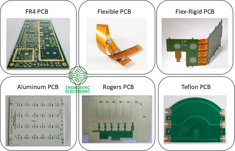
The PCB board could be rigid PCB, could be flex PCB and also could be Flex-Rigid PCB. And the materials could be FR4, PI, Aluminum, Copper-based, Rogers, Teflon, etc. They have different applications. For example, FR4 PCB is the most commonly used for rigid PCB and almost good for all electronics products; PI is the most commonly used for flex PCB; Aluminum and copper-based have good thermal diffusivity and always used for LED PCB ; Rogers PCB and Teflon PCB are always used for High Frequency PCB, etc.
PCB Manufacture Capabilities
|
Features |
Capabilities |
|
Layers |
1-36 layers |
|
Material |
FR-4, Aluminum, Copper, Polyimide, high frequency (Rogers, PTEE, PI), etc. |
|
PCB Type |
FR-4 Standard PCB , Aluminum PCB , Copper-based PCB, HDI PCB, Rigid-Flex PCB, Flex PCB, Thick Copper PCB and Rogers PCB, etc. |
|
Board Thickness |
0.1mm-6.0mm |
|
Copper Thickness |
1/2oz-6oz(18um-210um) |
|
Biggest Board size |
600mm*1200mm |
|
Min Tracing/Spacing |
0.075mm/0.075mm (3mil/3mil) |
|
Min drilling Hole diameter |
0.15mm(6mil), 0.1mm(4mil)-laser drill |
|
Solder Mask |
Green, Black, White, Red, Yellow, Blue and Purple, etc. |
|
Silkscreen color |
White, Blue, Black, Red, Yellow |
|
Surface finish |
HASL Lead free, Immersion Gold (ENIG), Immersion Tin, Immersion Silver, OSP, Carbon oil, etc. |
|
Special Techniques |
Impedance Control, Gold Fingers, Blind/Buried vias, Peelable solder mask, Half holes, Via-in-Pad and Countersink hole, etc. |
PCB Products Show

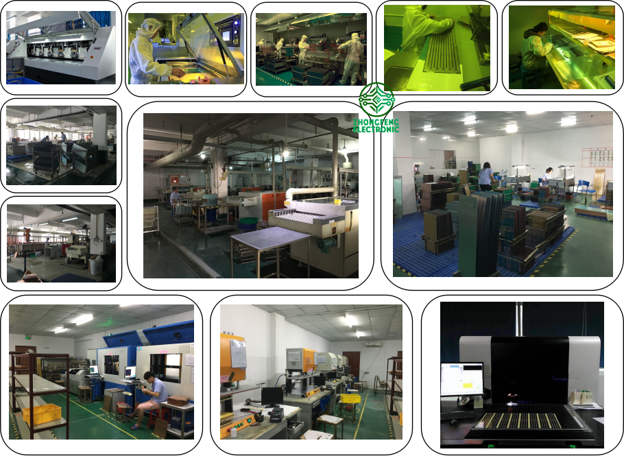
PCB Factory Show

HDI PCB
HDI PCB,HDI Microvia PCB,Prototype HDI PCB,HDI PCB Circuit Board
ZhongFeng Electronic Technology Co., Limited , http://www.1pcbassembly.com