Description: In this test, each bank is accessed only once, and then accesses other banks in turn. DDR3 has a limit on the number of Bank Open commands that can be input within a certain period of time, that is, only up to 4 Bank Open commands are allowed to be input within a certain period of time. At the same time, there are gap requirements between the line open commands of two consecutive banks. From the overall effect point of view, as long as the gap between the two banks is opened, the limit of only opening 4 banks in a certain period of time can be satisfied. These limits are inherently not subject to bandwidth loss as long as the scheduling is reasonable. However, due to the implementation of Xilinx's DDR3 controller, this limitation is almost doubled. The DDR3 controller can only open up to 4 banks at a time, and then must close the opened bank and then open the new bank. The resulting bandwidth overhead is also amazing. In this mode, the effective time is 32 ns, the invalid time is 48 ns, and the bandwidth utilization is 32/80 = 40% in the time taken by a set of write operations.
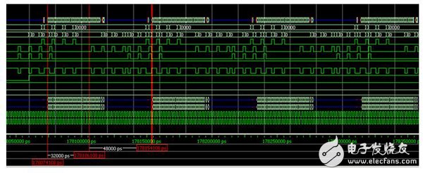
Figure 4 8 Bank access sequence diagram
IV.4Bank access test:Description: In this test, access to other banks in turn, using a total of 4 banks. After the four banks have finished accessing, they will access the four banks one by one, and the accessed addresses of the same bank are in the same row in the same row. Used to observe Xilinx management of Bank. The test scenario is basically similar to test item 3. The result shows that after issuing four Bank open commands, even if the next access is to open the opened bank of the Bank, the four banks that have been opened must be closed first, and the new bank is reopened. This bank management method is obviously simple, but it will greatly waste the bandwidth of DDR3. In this test item, the effective time length is 32 ns, the invalid time length is 48 ns, and the bandwidth utilization rate is 32/80=40%.
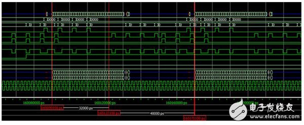
Figure 5 4Bank access sequence diagram
Nantong Boxin Electronic Technology Co., Ltd. , https://www.ntbosen.com