In the process of communication between the UAV system and the ground station, the contradiction between the high-speed generation of the on-board gyroscope attitude data and the transmission of the external relatively low-speed wireless data module is increasingly prominent, which seriously restricts the development of the UAV. Aiming at this problem, FPGA FIFO is used as high-speed data buffer, and a pre-machine communication interface of drone gyroscope based on FPGA built-in FIFO is proposed. Through the high-speed asynchronous FIFO buffer, the UAV gyroscope attitude data is sent to the ground station accurately via the FPGA, which significantly improves the data transmission quality and realizes the communication between the high-speed chip and the low-speed device. The whole design has good effect in practical application, the data is stable and reliable, meets the requirements of low error rate and high stability, and the demand of high-speed communication between drone and ground station, and has broad market application prospects.
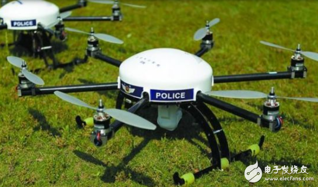
The UAV system has extremely high real-time, reliability and stability requirements for the control signals transmitted by the ground station and the attitude data returned by the aircraft. This poses a new challenge to the design of the UAV communication system. For UAV systems using ARM as a microprocessor, systems often need to coordinate the work between ARM processor-based high-speed gyroscope modules and relatively low-speed external wireless data transmission modules. Under the requirement of high communication stability and low bit error rate, the processor has to spend time running a null operation to wait for an external relatively low-speed transmission module to complete the reception/transmission of one frame of data. The processor computing cycle that is wasted by waiting for it virtually reduces the real-time nature of the entire flight control system, which in turn leads to many potential instability factors. This design combines the development needs of UAV system, adopts FPGA FIFO as high-speed data buffer, and proposes a pre-machine communication interface of drone gyroscope based on FPGA built-in FIFO. Through the high-speed asynchronous FIFO buffer, the UAV gyroscope attitude data is sent to the ground station accurately via the FPGA, which ensures the transmission quality and bridges the communication between the high-speed chip and the low-speed device.
The basic working principle of FPGA built-in FIFO
The FIFO is a FIFO queue, which adopts a ring storage circuit structure and is a traditional sequential execution method. The first-input instruction is completed and retired, and then the second instruction is executed. It is a first-in, first-out data buffer. According to whether the read/write clock frequency of the FIFO is the same, the FIFO can be divided into a synchronous FIFO and an asynchronous FIFO. The application of FIFO can well coordinate the communication of different clocks and different data width data to meet the high/low speed clock frequency requirements. Compared with ordinary memory, the FIFO has no external read/write address lines and is convenient to use.
The FPGA asynchronous FIFO is used to connect the ARM processor-based high-speed UAV gyro module with relatively low-speed wireless data transmission peripherals. From a hardware point of view, a FIFO is essentially a piece of data memory. The asynchronous FIFO uses two clock signals to control its read and write operations, which are the write clock (wrclk) and the read clock (rdclk). One is used to write data, that is, the data is stored in the FIFO; the other is used to read data, that is, the data is taken out of the FIFO. There are two pointers associated with the FIFO operation: the write pointer points to the portion of memory to be written; the read pointer points to the portion of memory to be read. The FIFO controller controls the movement of the two pointers by an external read/write signal, and thereby generates a FIFO null signal or a full signal. The read and write clocks are designed independently of each other, effectively ensuring asynchronous communication of data at both ends of the FIFO.
ARM-based drone gyroscope interface structure
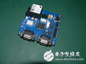
Due to the restriction of airborne fuel and electric energy reserves, unmanned aircraft equipment requires small size and light weight, and high energy efficiency ratio. Therefore, high requirements are placed on chip selection and circuit structure. Based on various factors such as comprehensive stability, data accuracy, operating temperature, package volume and energy consumption, the drone gyro sensor was strictly screened to determine the gyroscope scheme shown. The main control chip of the drone gyroscope uses the STM32F103T8 processor of the ARM 32 bit CortexTM M3 core. It has built-in 64 KB of flash memory and 20 KB of running memory, as well as 7 channels of DMA, 7 timers, 2 UART ports, and more. With an onboard 8 MHz crystal and an internal PLL from the STM32, the controller can run at 72 MHz and provides powerful hardware support for attitude resolution.
The triaxial acceleration and triaxial angular velocity sensor uses Invensense's MPU-6050 single-chip solution, the world's first integrated 6-axis motion processing component, eliminating the need for integrated gyroscopes and accelerometer axes compared to other multi-chip implementations. The problem of the difference between the two greatly reduces the packaging space. The three-axis magnetometer uses Honeywell's HMC5883L chip, which uses advanced high-resolution HMC188X series magnetoresistive sensors and industry-leading anisotropic magnetoresistance technology (AMR) for axial high sensitivity and linear high accuracy. The measurement range is from milli-Gauss to 8 Gauss, which is stable and reliable. The air pressure sensor uses Bosch's BMP180 chip, which has excellent performance, absolute accuracy of 0.03 hpa, and extremely low power consumption. The sensor is housed in a powerful 7-pin ceramic leadless chip carrier (LCC) ultra-thin package for easy installation and use. Each sensor and ARM processor are connected by I2C bus, as shown in Figure 3.
FPGA FIFO and gyroscope connection
In combination with the characteristics of the UAV ARM gyroscope, in order to adapt to the complexity of the process and realize the simplicity of operation, the design selected Altera's CycloneII series chip EP2C8Q208C8N, Verilog code design on the Quartues II platform, using the FIFO IP core provided by Altera Corporation . This solution is stable and efficient and easy to develop.
Gyro connection to FIFO and FPGA
The processor collects the sensor signals and performs attitude calculation inside the ARM to obtain pitch angle, roll angle, heading angle, air pressure, altitude and temperature information. In order to send the solved data back to the ground station in time, the processor controls the write request signal wrrq and the write clock wrclk to write the data to the FIFO at high speed, and then returns to the flight control program to perform the attitude calculation for the next cycle. After the FIFO is full, the full-flag bit wrfull will be set high. The ARM processor determines whether to continue writing data by detecting the status of the full flag. At the same time, it is judged whether or not to continue reading data in the FPGA by detecting whether the read FIFO is the empty flag bit rdempty. The read empty flag bit is low level to indicate that there is data in the FIFO, which can be read, and the data is read in time with the read request signal rdreq and the read clock rdclk until the data is completely read out, and the flag bit changes to a high level. There is no data in the FIFO. The connection between the ARM-based gyroscope and the FIFO and FPGA is shown in Figure 4.
Organic Light Emitting Diode,Pm Oled,Oled For Medical Products,Stepper Motor Oled
ESEN Optoelectronics Technology Co., Ltd, , https://www.esenoptoelectronics.com