Yan Yanbin, Jiang Zhiyu, Zhang Baoning, Nanjing Institute of Electronic Technology
Keywords: RapidIO protocol; exchange; field programmable gate array; VPX bus; master
0 Preface
The rapid development of radar systems, the large amount of radar signal processing operations, and the complex algorithm structure require signal processing systems to be capable of high-speed, real-time, high-performance, and flexible completion of various processing tasks. For signal processing system processors, processing capacity, system data bandwidth, and systems The reconfigurable capabilities put forward higher requirements. The RapidIO protocol is an open peer-to-peer packet switching standard. It can provide a high-bandwidth, low-latency, high-reliability data channel while supporting a distributed global shared storage system that maintains Cache consistency by hardware and uses the interconnection protocol RapidIO. The construction of a new radar signal processing system based on a crossbar switch is a good design solution. The RapidIO protocol is a high-performance, low-latency, high-efficiency, system-level interconnect protocol based on packet switching. It has higher transmission efficiency than 10 Gigabit Ethernet and PCIe and can meet the needs of embedded system applications. VPX (VITA46) bus is a new generation bus standard based on high-speed serial bus. It is a major innovation to the traditional VME bus, supports data exchange system architecture, and is compatible with high-speed serial bus protocols such as Fiber Channel, PCI Express, RapidIO, and Hypertransport. , and inherited the mechanical structure of the VME standard and the advantages of cooling and seismic resistance.
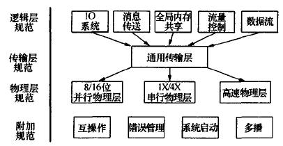
The RapidIO protocol hierarchy is shown in Figure 1.

Figure 1 RapidIO protocol hierarchy
The logic layer specification defines the operation and related transactions between nodes. The generic transport layer defines how transactions are routed from one node to another through a switch. The physical layer defines how two adjacent processing units are electrically connected. RapidIO packets are formed by a combination of bit fields defined by the logic layer, the general transport layer, and the physical layer.
1 Technical parameters of RapidIO switching
The main technical indicators of the exchange design are as follows:
1) Support RapidIO 1.3 standard, physical layer 4X serial RapidIO;
2) Support 16-way 4X RapidIO full exchange, single data rate l0 Gbps, total bandwidth 160 Gbps;
3) RapidIO data transmission error rate is less than 10-12;
2 RapidIO Switched FPGA Architecture and Device Selection
As can be seen from the RapidIO protocol hierarchy shown in Figure 1, the RapidIO switch is unpacked and exchanged at the transport layer. Therefore, in the field programmable gate array (FPGA), only the transport layer, physical layer, and additional specifications need to be implemented. Implement the logic layer. In this design, the best choice of FPGA is XILINX's Virtex5 series, the specific model selection XC5VTX240T. The XC5VTXT series is designed for a large number of high-speed serial interconnects. The XC5VTX240T has 48 high-speed serial interfaces that are particularly suitable for RapidIO switching designs.
This design needs to implement 16 channels of 4X RapidlO full exchange, and it needs to implement sixteen 4X RapidlO physical layer endpoints and the switching logic between each endpoint. Since 16 RapidIO endpoints need to occupy a large amount of FPGA resources, the capacity of XC5VTX240T has been exceeded. This design uses two XC5VTX240Ts to implement the two XC5VTX240T channels with sufficient bandwidth to satisfy the RapidIO switching requirements between each other. The following describes the actual RapidIO switch module.
3 RapidIO Switch Module Configuration
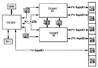
Figure 2 shows the system block diagram of the switch module.

Figure 2 Block Diagram Based on VPX Bus RapidIO Switching Module
As shown in Figure 2, this module uses a VPX bus. The main function is implemented by three Xilinx Virtex5 series FPGAs: 2 XC5VTX240T and 1 XC5VFX100T (hereinafter abbreviated as TX240T and FX100T respectively). The 2xTX240T realizes the 4X RapidIO switching function for external l6 channels, and the FX100T implements the RapidIO system management and configuration functions.
3.1 TX240T Function and Architecture
The external RapidIO interface of the VPX RapidIO switch module is provided by two TX240Ts. The TX240T implements RapidIO's main functions such as data unpacking, buffering, routing, arbitration, and data flow control.
The TX240T is the main bearer of the switch. It internally consists of RapidIO receiving logic, receiving buffer queues for each port and channel, switching switches, packet queue priority scheduling logic, sending buffer queues for each port, flow control logic, and RapidIO sending logic. After the TX240T receives the data packet, it unpacks the data according to the RapidIO protocol. The data packet type is determined first. If it is a maintenance packet, the data packet is sent to the FX100T through the LVDS data channel between the TX240T and the FX100T; if it is an ordinary data packet The end point of the data packet is obtained, then the query routing table is exchanged, the packet route is determined according to the destination end point, and the destination port is determined to be sent. When the source VI and destination port of the RapidlO packet belong to the same chip TX240T, the data packet is directly output from another port through the internal switching network of the TX240T; when the source port and the destination port of the RapidIO packet do not belong to the same chip TX240T, the data The packet first passes through the internal switching network of the first TX240T and is transmitted to another TX240T via the data channel between the two TX240Ts. The packet is then sent to the output port through the internal switching network.
3.2 FX100T Function and Architecture
The FX100T mainly implements the RapidIO system initialization configuration, system operation management, and backup function support for the switch module.
The main components of the FX100T include the PowerPC processor, maintenance engine, and switch. FX100T embedded PowerPC processor hard core, used as the entire module control and processing unit. The FX100T is responsible for the operation of all maintenance packages for the exchange module, parsing the maintenance package, and then doing the related register operations. The maintenance engine is responsible for processing the CPU-initiated maintenance package for configuring each port and the CPU-initiated direct operation register request.
4 data channels
The external RapidIO interface of the VPX RapidIO switch module is provided by the TX240T. When the source and destination ports of the RapidIO packet belong to the same TX240T, the data packet is directly output from another switch through the internal switching network of the TX240T. When the source port of the RapidIO packet is used When the destination port does not belong to the same TX240T, the data packet first passes through the internal switching network of the first TX240T, passes through the interrogating data channel, and is transmitted to another TX240T, and then to the output port through the internal switching network.
This module provides RapidIO system management function, which is provided by FX100T. There are two independent LVDS configuration packet data channels between FX100T and 2 TX240T. Maintenance packages configured and managed for other RapidIO endpoint modules are sent by the FX100T, sent to the TX240T through the configured channel, and then sent to the corresponding RapidIO port for transmission via the TX240T internal switching network.
5 RapidIO Packet Operation Flow
The RapidIO protocol hierarchy includes the physical layer, transport layer, logic layer specifications, and additional specifications. The logic layer specification defines the operation and related transactions between nodes. The generic transport layer defines how transactions are routed from one node to another through a switch. The physical layer defines how two adjacent processing units are electrically connected. RapidIO switching is performed at the transport layer for unpacking and switching. Therefore, only the transport layer, physical layer, and additional specifications need to be implemented in the FPGA, and there is no need to implement the logic layer.
5.1 RapidIO Packet Reception
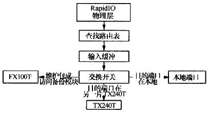
The receiving process of each RapidIO packet is the same, as shown in Figure 3.

Figure 3 RapidIO packet receiving process
The receiving part of the RapidIO switch receives the data packet through the physical layer of the RapidIO protocol, and at the same time, decomposes the data packet and stores the routing information in the storage structure. The receiving part uses an input buffer to buffer the received data. According to the routing information in the storage structure, the data packet is forwarded to the corresponding port of the TX240T and another corresponding port of the TX240T or FX100T.
5.2 RapidIO data transmission
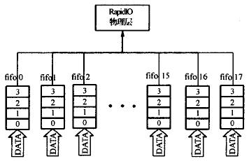
Figure 4 shows the structure of the sending part. The role of the RapidIO data sending part is to send the received data over the link. Each port may receive 8 4X RapidIO data from this block TX240T, 8 4X RapidIO data from another TX240T, and 2 4X RapidIO data from FXIOOT, a total of 18 4XRapidIO data, 18 buffered data sent after arbitration Send the RapidIO physical layer IP core to other RapidIO endpoints.

Figure 4 sender structure
6 actual test
The test of this module uses general-purpose company's processing module DSP230, DSP230 module uses 4 pieces of 8641D processors, each processor embedded in RapidIO endpoints. Each RapidIO endpoint is in 4x mode, with a baud rate of 3.125 Gbps, data bandwidth of 10 Gbps, and four RapidIO endpoints connected to the RapidIO switch chip (Tsi578) on the board. The module externally derives RapidIO interfaces from the switch chip.
After testing, this module implements the RapidIO master control function, successfully initializes each RapidIO endpoint of the DSP230 and the Tsi578, and exchanges various RapidIO packets sent by the DSP 230 to each port. The data bandwidth meets the requirements.
7 Conclusion
This article combined with the specific RapidIO switch module design, illustrates a Xilinx company's FPGA chip to achieve multi-port, large-scale RapidlO exchange design. After actual measurement, this module successfully implemented the exchange of RapidIO packets with a bandwidth of 10 Gbps and initialized and managed the entire RapidIO system. This module is applied to the actual radar system and has achieved good results.
Window Optical Lenses,Optical Lenses,Window Optical Lens,Calcium Fluoride Glass Window
Danyang Horse Optical Co., Ltd , https://www.dyhorseoptical.com