1 Introduction
A digital storage oscilloscope is different from a general analog oscilloscope. It converts the acquired analog voltage signal into a digital signal, which is analyzed, processed, stored, displayed, or printed by an internal microprocessor. These oscilloscopes usually have program control and remote control capabilities, and the GPIO interface can also transfer data to an external device such as a computer for analysis and processing. With the continuous development of large-scale integrated circuits, the powerful DSP digital signal processor is becoming more and more real-time. With its powerful digital signal processing capability, DSP provides a reliable and practical platform for the implementation of data acquisition systems for digital oscilloscopes, and improves the sampling rate, memory depth, and waveform capture capabilities of digital storage oscilloscopes.
The digital storage oscilloscope described herein is a DSP-based dual channel digital storage oscilloscope. The oscilloscope uses TI's TMS320F2812 chip, which features high-speed digital signal processing and filtering, real-time, large-capacity waveform storage, and fast signal processing. And the digital storage oscilloscope has the advantages of being portable, simple in operation, high in accuracy, and large in sampling rate.
2. Overall design
The digital oscilloscope is mainly composed of a front-end voltage stabilization processing circuit, an AD conversion circuit, a NIOS system integrated in the FPGA chip, various control circuits and SDRAM, various keyboards and an LCD interface. The DSP chip used as the core of the back-end processing is TI's TMS320F2812. It is a 32-bit fixed-point DSP chip with 128K*64-bit on-chip flash memory 18K*16-bit data/program memory and 4K*16 bits. Boot Rom, the FPGA chip as the front-end acquisition control processor, uses Altera's EP2C5Q208, which is a low-cost FPGA chip in the Cyclone series with up to 119,808 bits of internal RAM, 4,608 logic cells, supporting Altera's NIOSII And SOPC to meet the design requirements.
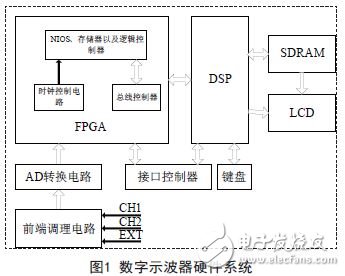
As shown in Figure 1, the measured signal is first from channel 1 or channel 2. Since the amplitude of the analog signal received by the two channels is in an unstable state, it must be processed by the conditioning circuit to be a voltage range that the A/D conversion circuit can receive. Otherwise it will cause very serious consequences. The A/D conversion circuit can convert the conditioned analog signal into a digital signal after being sampled, held, quantized, encoded, etc., and sent to the FPGA chip under the action of the SDRAM controller. Under the overall control of the built-in NIOS of the FPGA, the internal FIFO is used for buffering and corresponding data processing.
In this design, the DSP is the core of the entire oscilloscope data processing and display, performs the main data processing, and outputs the processing results and corresponding control signals. The FPGA works under the control signal sent by the DSP. The DSP is a high-speed digital signal processor. The data processed by the FPGA and stored in the buffer memory is sent to the original buffer in the SDRAM under the action of the DSP control signal. After being processed by various algorithms such as DSP difference and filtering, it is sent to the display buffer of the oscilloscope card for waveform display on the LCD screen.
2.1 Front-end conditioning circuit and A/D sampling design
The general A / D chip allows the input voltage amplitude to be fixed (-0.5v ~ +0.5v), the pre-processing circuit consisting of various signal attenuation and amplification and voltage bias network, is responsible for receiving the front end The stabilized analog signal is stabilized within the allowable input voltage range after the method and attenuation. Generally speaking, the front-end pre-processing circuit consists of two parts. One is an attenuation network composed of a relay and an RC, which can avoid the distortion of the signal and facilitate the reference adjustment of the digital storage oscilloscope; the second is by two op amps. The AD8008 consists of a resistor-capacitor matching network and a driver amplifier circuit. The AD8008 is a dual-channel, high-performance, current-feedback amplifier with ultra-low distortion and noise characteristics, a bandwidth of 650MHz, and a wide supply voltage range (5V~12V).
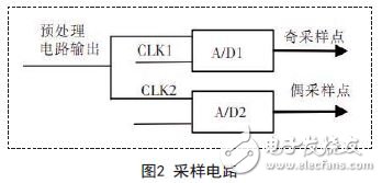
The core of data acquisition is the A/D conversion function. Although the DSP chip itself has the function of A/D conversion, in order to improve its working speed, this design uses two AD9288 to complete the analog-to-digital conversion. Under the control of the sampling clock, it forms a phase difference of 180 degrees, which satisfies the sampling rate of 200 MS/s.
The AD9288 is a dual-core, 8-bit, single-chip sampling analog-to-digital converter with on-chip sample-and-hold circuitry for low cost, low power, small size, and ease of use. The AD9288 operates at 100MSPS slew rate and delivers outstanding dynamic performance over the entire operating range. The output of the AD9288 is a binary code that can be stored directly after being sent to the FPGA memory module. Each channel can work independently up to 475MHz analog bandwidth, allowing dual channels to work in parallel.
2.2 Trigger circuit
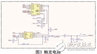
The trigger circuit is an important function circuit of the signal acquisition system. Its basic function is to provide a stable trigger phase point, which is used as the time reference zero point of the horizontal scanning time base, so that the waveform is stably displayed on the display screen. The acquisition circuit design realizes a trigger pulse signal related to the measured signal in one cycle, and controls the ADC data acquisition.
The core component of the trigger circuit is a high-speed level comparator. The AD96685 chip and the LT1713 chip are used in this acquisition circuit. The trigger circuit is shown in Figure 3. The TrigLevel signal is the comparison level at which the low frequency component of the source signal is superimposed, Ref is the reference potential, and the Trig Source signal is the source signal that is triggered. The adjustment of the trigger level is achieved by changing the level value of the Trig Level signal. After pairing by LT1713, a pair of ECL differential clocks, TrigP and TrigNP, are output, and then level-converted and sent to the trigger in the FPGA.
UV Film,UV Screen Protector,UV Curing Screen Protector
Shenzhen Jianjiantong Technology Co., Ltd. , https://www.tpuprotector.com